
This guide is written for engineers and technical teams building connected devices who need clear, field-ready guidance without getting lost in standards documentation.
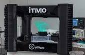
Nano-Ops is commercialising an automated wafer-based process and fab-in-a-box based on the directed assembly technology which can 'print' features down to 20nm.
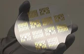
Here, In the first step a pattern is first etched into a template wafer.
To scale up microLED displays to large areas, smaller displays can be titled. Because microLEDs can be truely edge-less devices, the tiling can function, yielding a seemless look.
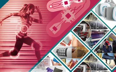
Stretchable Electronics and inks for durable wearable electronics. These inks can be printed on TPU films which can be bonded to fabrics. This results in devices that stretch without cracking and maintain excellent electrical properties. Examples include biometric sensors & fixed resistance heaters
An instrumentation amplifier is a precision differential amplifier designed to amplify small voltage differences. This guide explains the three-op-amp architecture, and how to choose between INA128, AD620, LT1167, and a standard difference amplifier for sensor front-ends.
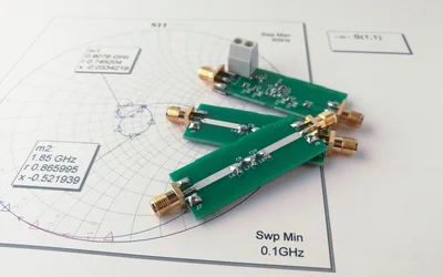
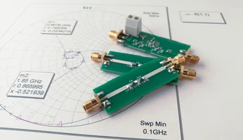
A guide covering the full radio-frequency design workflow, starting from setting specifications and choosing topologies to matching, simulation, layout, and verification, to help antenna engineers.
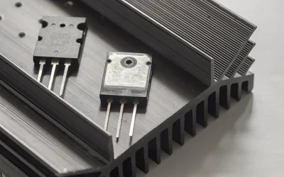
This article presents a detailed technical exploration of SiC MOSFET devices, covering material physics, device structure, switching behavior, and practical design considerations for high-efficiency power electronics systems.
This article is a comprehensive technical guide to relay wiring diagrams, covering 4-pin and 5-pin configurations, working principles, safety practices, standards, and advanced relay applications in modern systems.
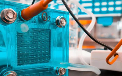
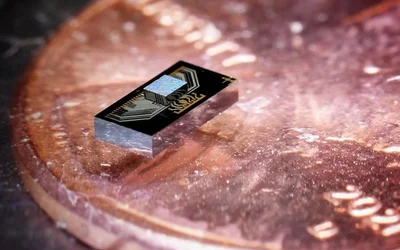
The integrated design achieves accurate micro gas chromatography and can help reduce the cost of monitoring chemical synthesis, natural gas pipelines or at-home air quality.
Hybrid bonding provides the adhesive free, copper to copper interconnects that are driving cutting edge 3D chip stacking. This article explains the theory, process, benefits, challenges, applications, and emerging trends of hybrid bonding for engineers.
Nano-Ops is commercialising an automated wafer-based process and fab-in-a-box based on the directed assembly technology which can 'print' features down to 20nm.
Here, In the first step a pattern is first etched into a template wafer.
To scale up microLED displays to large areas, smaller displays can be titled. Because microLEDs can be truely edge-less devices, the tiling can function, yielding a seemless look.
Stretchable Electronics and inks for durable wearable electronics. These inks can be printed on TPU films which can be bonded to fabrics. This results in devices that stretch without cracking and maintain excellent electrical properties. Examples include biometric sensors & fixed resistance heaters
Silver nanoparticle inks improve every year. These improvements are often incremental, but very important. One ever-present direction of development is towards inks which offer ever higher conductivity levels at a low curing temperature and a short curing time. This a critical figure of merit because it opens more substrate choices, saves time, and lowers energy consumption costs.
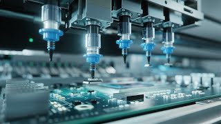
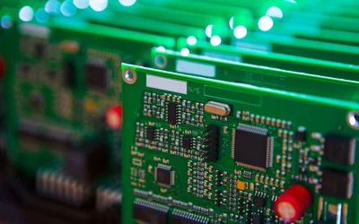
Circuit card assemblies (CCA) give birth to a complete printed circuit board (PCB) after assembling every component. A printed circuit board has no electrical components and needs to go through a manufacturing process called circuit card assemblies which are the complete board assembly.
Carnegie Mellon University collaborators pioneer the CMU Array—a customizable, 3D nano-printed, ultra-high-density microelectrode array platform for next-generation brain-computer interfaces. This technology can transform the way doctors are able to treat neurological disorders.

Printed batteries offer thinness and flexibility, enabling new applications, but their production is deceivingly complex. Gunter Hübner from Stuttgart Media University offered some insights at the e-Swiss conference last week.
Experimenting in the world of Flexible Hybrid Electronics (FHE) comes with a variety of hurdles. Printing technologies are vastly different in terms of materials compatibility and have pros and cons that make them suitable for particular applications. Choosing materials that match the printing technology you intend to use is the most important decision you’re going to make.


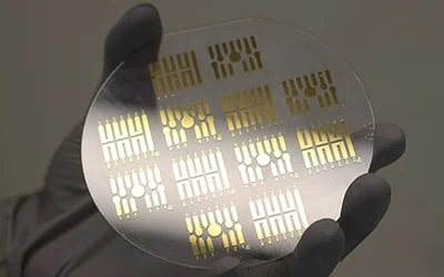
But what if one could print, digitally, using any paste and ink on any substrate? Read more
Researchers have designed smart, colour-controllable white light devices from quantum dots, tiny semiconductors just a few billionths of a metre in size, which are more efficient and have better colour saturation than standard LEDs, and can dynamically reproduce daylight conditions in a single light
If the transition to renewables is to succeed, we will need a viable means of storing surplus heat and electricity. Globe spoke to experts from ETH Zurich about the promising technologies that could help us reach net zero.
The collaborative nature of open source projects brings together people across the world to work towards improving and monitoring our natural resources.