SiC MOSFET: Wide-bandgap Power Devices for High-Efficiency Converters
This article presents a detailed technical exploration of SiC MOSFET devices, covering material physics, device structure, switching behavior, and practical design considerations for high-efficiency power electronics systems.

20 Apr, 2026. 14 minutes read
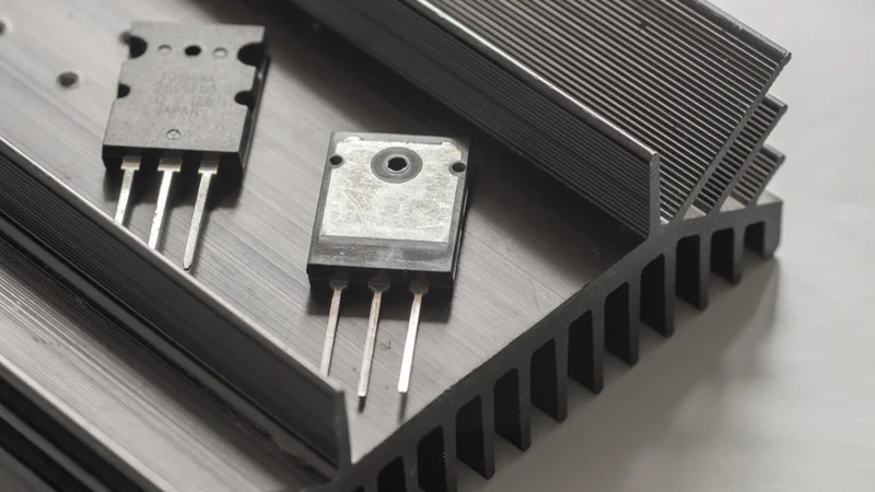
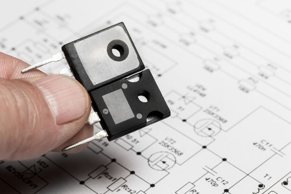
Two High-Power MOSFET Transistors Packaged in a TO-247 Case
Key Takeaways
Wide-Bandgap Advantage: Silicon carbide (4H-SiC) offers a 3.26 eV bandgap, enabling SiC MOSFETs to achieve higher breakdown strength, improved thermal conductivity, and superior performance over silicon-based power semiconductors.
Low On-Resistance & High Voltage: Modern SiC MOSFETs deliver very low drain-source on-resistance while supporting high blocking voltage, making them ideal for high-power power converters and inverters.
High-Temperature Operation: Advanced silicon carbide technology supports junction temperatures up to 175–200°C, enabling reliable operation in demanding automotive and industrial power electronics environments.
Gate-Drive Requirements: Proper gate-drive design is critical, with typical gate-voltage ranges of +15 V to +20 V and optional negative bias for stable, fast switching and reduced switching losses.
Automotive-Grade Reliability: Many SiC power devices comply with AEC-Q101, JEDEC, and IEC standards, ensuring robust performance in harsh conditions and long-term reliability.
Broad Applications: SiC MOSFETs are widely used in electric vehicle systems, chargers, solar inverters, industrial drives, and data-center power supplies, enabling efficient and compact power conversion solutions.
Introduction
Demand for higher efficiency in electric vehicles, renewable energy systems, and data-center power supplies is accelerating the transition to advanced power semiconductors. Traditional silicon IGBTs or super-junction MOSFETs are constrained by intrinsic material limits, including a narrow bandgap and a lower critical electric field. In contrast, wide-bandgap materials such as silicon carbide enable superior performance across voltage, switching speed, and thermal domains. SiC MOSFETs are now commercially viable and cost-competitive, enabling traction inverters that push EV efficiency while reducing system weight and heat sink requirements.
Modern SiC MOSFET technology supports compact, high-frequency converter designs with improved power density and reduced cooling requirements. Today, the SiC MOSFET is becoming central to next-generation inverter and converter architectures. This article presents a detailed technical exploration of SiC MOSFET devices, covering material physics, device structure, switching behavior, and practical design considerations for high-efficiency power electronics systems.
Wide-Bandgap Semiconductor Physics
Silicon Carbide (SiC) is a compound semiconductor composed of silicon and carbon, widely used in modern power semiconductors due to its superior material properties.
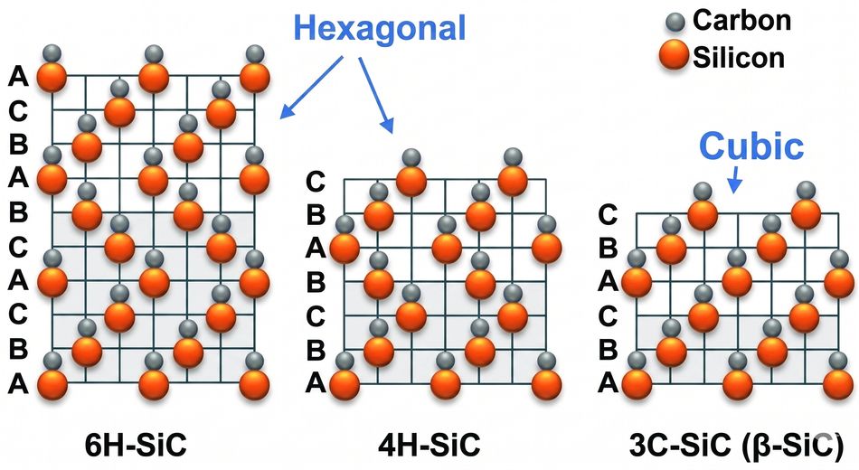
The 4H-SiC polytype, dominant in silicon carbide MOSFET fabrication, exhibits a bandgap of approximately 3.26 eV, nearly three times that of silicon (1.15 eV). [1] Moving electrons from the valence to the conduction band, therefore, requires more energy, meaning intrinsic carrier concentrations remain extremely low even at high temperatures. This wide bandgap leads to several important properties:
High Critical Electric Field: 4H-SiC sustains breakdown fields of ~2.5–3 MV/cm, compared to ~0.3 MV/cm for silicon. Devices can be designed with thinner drift regions, resulting in lower on-resistance at a given breakdown voltage.
Superior Thermal Conductivity: The thermal conductivity of SiC is about 4.9 W/(cm·°C), over 3 times that of silicon, facilitating efficient heat dissipation. Heat generated during switching is removed more quickly, enabling smaller heat sinks and higher power density.
Saturation Velocity: Carriers in SiC achieve higher saturation velocities (~2 × 10⁷ cm/s) than in silicon, allowing faster switching and reduced conduction losses. [2]
High Temperature Capability: The intrinsic carrier density of SiC remains low until temperatures exceed 800°C, enabling devices with junction temperature ratings of 175°C to 200°C.
These material advantages permit SiC MOSFETs to combine the normally mutually exclusive attributes of high breakdown voltage, low on-resistance, and fast switching. The carrier mobility in SiC (900 cm²/V·s for electrons) is lower than that of silicon; the dominant factor influencing the drain-source on-resistance is the cube dependence on the critical electric field.
Recommended Reading: Silicon Carbide (SiC) Wafers: Revolutionizing Power Electronics and Beyond
SiC MOSFET Device Structure
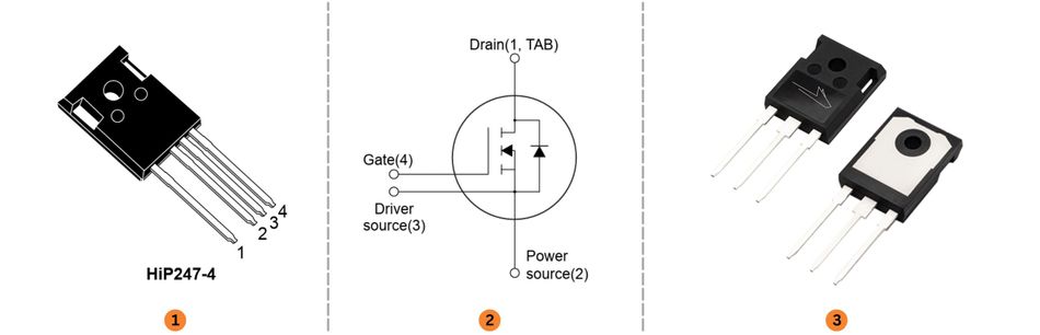
SiC MOSFET consists of an N-type drift layer grown on a heavily doped N+ substrate, with a P-well forming the channel and an N+ source implant.
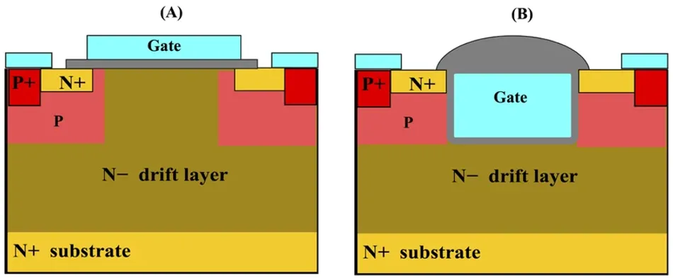
The two main gate structures used are:
Planar Gate: Early SiC MOSFETs employed planar structures in which the gate oxide lies on the semiconductor surface. These devices offer robust short-circuit capability and simpler wafer-level fabrication. However, a higher interface trap density increases channel resistance, thereby impacting the overall on-resistance.
Trench Gate: Modern devices use trench structures, in which the gate is embedded in the drift region. This reduces channel length, lowers drain-source on-resistance, and increases cell density, improving power density. Advanced trench designs also reduce electric-field stress on the oxide, enhancing long-term reliability under high-gate-voltage operation.
Most discrete SiC MOSFETs include an intrinsic body diode formed by the P-well and N-drift region. Unlike silicon diodes, SiC body diodes exhibit fast reverse-recovery and can operate at high temperatures, enabling synchronous rectification without additional antiparallel diodes. Some manufacturers co-package a SiC Schottky diode with the MOSFET to further reduce reverse recovery losses in hard-switching topologies.
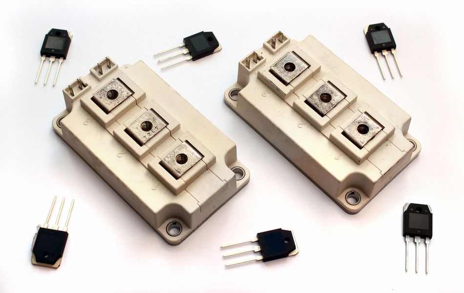
SiC MOSFETs are offered in voltage classes from 650 V (targeting server power supplies and solar inverters) up to 1,700 V for traction and rail applications. The packages include through-hole TO-247-3/4, HiP247-4, TO-263-7 (D2PAK-7L) and surface-mount PG-HSOF-8 and TOLL packages. Many devices feature a Kelvin source pin to isolate the gate-drive return and minimise parasitic inductance, thereby improving switching speed and dV/dt immunity.
Recommended Reading: How Does a Diode Work: Unraveling the Heart of Electronic Control
Switching Performance
On-state Resistance and Conduction Losses
The superior wide-bandgap properties of silicon carbide enable SiC MOSFETs to achieve extremely low on-resistance at high blocking voltage levels. Unlike silicon-based power MOSFETs, where drift-region resistance dominates, SiC power devices benefit from a higher critical electric field, enabling thinner drift layers and lower conduction resistance.
Devices such as the Wolfspeed C3M0032120K (1200 V) exhibit a typical drain-source on-resistance of around 32 mΩ, while alternatives from onsemi and Infineon show similar low-loss characteristics across various power modules. Even planar MOSFET technology solutions maintain competitive performance, although trench structures further reduce resistance and improve power density.
The conduction losses follow:

This relationship highlights how reduced on-resistance directly lowers power dissipation in high-power converters and inverters. Compared to IGBTs, which rely on bipolar conduction and exhibit higher voltage drops, SiC MOSFETs enable higher-efficiency operation in electric-vehicle traction systems, chargers, and DC/DC converters. Additionally, the relatively stable temperature coefficient of drain-source on-resistance ensures predictable performance across high-temperature operating conditions.
Switching Losses and Reverse Recovery
The intrinsic body diodes in silicon carbide MOSFET devices exhibit very low reverse-recovery charge, unlike traditional silicon-based diodes. This reduces current overshoot, minimizes switching losses, and improves efficiency in hard-switching topologies such as PFC stages, AC/DC front ends, and DC/DC converters. In many designs, external Schottky diodes are either minimized or eliminated.
In contrast, IGBTs exhibit significant tail currents during turn-off due to minority-carrier recombination, leading to higher energy losses and limiting switching frequencies to tens of kilohertz. SiC MOSFETs, however, can operate efficiently at switching frequencies ranging from 100 kHz to 500 kHz, enabling smaller passive components, reduced inductance, and improved system-level power density.
Comparison With Silicon Devices
Once compared with traditional power semiconductors, SiC MOSFETs clearly outperform both silicon MOSFETs and IGBTs across key metrics. The lower drain-source on-resistance reduces conduction losses, while faster switching significantly lowers dynamic losses in power electronics systems.
Unlike silicon MOSFETs, which suffer from slow body diodes and high reverse recovery, SiC MOSFETs integrate fast intrinsic diodes with minimal charge storage. This reduces voltage spikes, lowers electromagnetic interference (EMI), and simplifies PCB layout and gate driver design.
Furthermore, the ability of SiC MOSFETs to operate at higher switching frequencies enables advanced topologies, including resonant and soft-switching power conversion architectures. These advantages translate into smaller system size, improved efficiency, and enhanced reliability in applications ranging from power supplies to automotive inverters and high-voltage industrial systems.
Thermal Characteristics and Reliability
One of the key advantages of SiC MOSFETs is their ability to operate at elevated junction temperatures. Commercially available devices have guaranteed operating ranges of 150°C to 200°C, significantly higher than those of typical silicon-based power semiconductors. For example, the C3M0032120K is rated up to 175°C junction temperature and can sustain high currents with a power dissipation of 283 W at 25 °C. SCT070W120G3-4 pushes the operating junction range to 200 °C and provides a typical thermal resistance of 0.74 °C/W, enabling high power density designs.
The high thermal conductivity of silicon carbide (~4.5–4.9 W/cm·K) allows efficient heat spreading across the die, reducing localized hotspots and improving overall thermal stability. [3] However, real-world thermal performance is often constrained by power modules, packaging, and interconnect technologies rather than the semiconductor itself. Parasitic inductance, PCB layout, and thermal interface materials also influence heat dissipation and switching behavior, particularly at high switching frequencies.
To fully leverage the performance of SiC MOSFET, designers must carefully evaluate datasheet parameters such as junction-to-case thermal resistance, derating curves, and safe operating area. Advanced cooling strategies, including double-sided cooling and top-side heat extraction, are increasingly used in automotive inverters, electric vehicle drivetrains, and high-voltage power electronics systems.
The reliability of SiC power devices is validated by rigorous qualification standards. AEC-Q101 ensures robustness in automotive applications through stress tests such as high-temperature reverse-bias, temperature cycling, and ESD. JEDEC standards like JESD22 and J-STD-020 address environmental and reflow reliability, while IEC standards (e.g., IEC 60747 and IEC 60068) evaluate performance under thermal, mechanical, and humidity stress.
These qualification frameworks ensure that SiC MOSFETs maintain long-term reliability in demanding environments. This makes them ideal for solid-state power conversion systems requiring durability, efficiency, and consistent performance.
Gate-Drive Requirements
SiC MOSFETs require specific gate-drive voltages and careful dV/dt management to realise their full performance. The important considerations include:
Gate Voltage Levels: Most silicon carbide MOSFET devices require a positive gate voltage of +15 V to +18 V for full enhancement and minimal drain-source on-resistance. Typical datasheet limits range from -4 V to +15 V (Wolfspeed) and up to +20 V (onsemi). Exceeding these limits risks damaging the gate oxide, a critical reliability concern in wide-bandgap semiconductor devices.
Negative Turn-Off Bias: To prevent false turn-on caused by high dV/dt during fast switching, designers often apply a negative bias (-2 V to -5 V). This helps discharge capacitance, particularly the Miller capacitance, ensuring robust turn-off in high-speed power converters, inverters, and PFC stages.
Gate Charge and Driver Capability: Compared to silicon devices, SiC MOSFETs typically exhibit lower gate charge, enabling faster turn-on and reduced driver losses. However, rapid transitions increase sensitivity to parasitic inductance in the PCB, potentially causing ringing and EMI. Using a Kelvin source connection and optimized gate driver circuits is critical for stable operation. The gate resistors must be carefully selected to balance switching speed, switching losses, and electromagnetic interference.
Miller Plateau and Switching Behavior: The Miller plateau in SiC MOSFETs typically occurs around 8–10 V, requiring sufficient driver current to maintain fast transitions. Switching times are often in the tens of nanoseconds, supporting high-frequency topologies in DC/DC converters and AC/DC systems.
Protection Features: Due to shorter short-circuit withstand times (~1–2 µs) compared to IGBTs, protection is critical. Advanced gate driver ICs incorporate desaturation detection, under-voltage lockout, and soft turn-off mechanisms. These features ensure safe operation of SiC power devices in demanding automotive, high-voltage, and high-power electronics environments.
Applications of SiC MOSFETs
EV Traction Inverters and Onboard Chargers
The electric vehicle ecosystem demands compact, high-efficiency power converters capable of handling hundreds of kilowatts. SiC MOSFETs enable inverters to operate at higher switching frequencies (>30 kHz), reducing motor torque ripple and shrinking passive components such as inductors and capacitors. This directly improves system-level power density and efficiency.
In automotive traction systems, silicon carbide MOSFETs reduce both switching and conduction losses compared to IGBTs, enabling improved thermal performance and extended driving range. Their high-temperature capability also enables tighter integration of power modules within motor housings. Leading EV manufacturers now widely adopt SiC power devices in traction inverters, DC/DC converters, and onboard chargers.
The onboard chargers benefit from fast switching and high blocking voltage, supporting advanced topologies such as LLC resonant and PFC stages. This enables efficiencies exceeding 98% in both single-phase and three-phase AC/DC power conversion systems. [4]
Solar Inverters and Energy Storage Systems
In photovoltaic systems, SiC MOSFETs significantly enhance performance in string inverters by reducing switching losses and enabling higher switching frequencies. This allows smaller magnetics and improved maximum power point tracking (MPPT) efficiency. Their capability to handle high-voltage DC bus levels (1000 V–1500 V) makes them ideal for modern solar farms.
In energy storage, DC/DC converters using silicon carbide benefit from the low reverse-recovery of intrinsic diodes, improving efficiency for bidirectional energy flow between batteries and the grid. This is critical in renewable integration and grid stabilization.
Industrial Motor Drives and UPS
The industrial power electronics applications, including motor drives operating at 400–690 V AC/DC, leverage SiC MOSFETs for reduced losses and higher efficiency. Increased switching frequencies allow compact designs and improved control accuracy.
In power supplies, SiC MOSFETs enable transformer-less topologies, reducing system size and weight. Their robustness and thermal performance also make them suitable for demanding applications such as welding systems, induction heating, and high-power industrial drives.
Data Center Power and DC Microgrids
The modern data centers require efficient power conversion to reduce operational costs. SiC MOSFETs improve efficiency in both AC/DC and DC/DC converters, minimizing energy losses and cooling requirements.
They also support emerging DC microgrid architectures (400 V–700 V DC), eliminating multiple conversion stages. This improves reliability and reduces system complexity in dense server environments, where high-temperature operation and compact PCB designs are critical.
Rail Traction and High-Voltage Converters
In rail and heavy high-power systems, SiC MOSFETs rated up to 1700 V provide a high-performance alternative to conventional IGBTs. Their ability to switch faster reduces the size of transformers and filters in traction power converters, improving efficiency and weight.
Additionally, SiC power devices enable efficient regenerative braking and are increasingly used in medium-voltage drives and solid-state transformer architectures. These capabilities make them essential in next-generation high-voltage power electronics for transportation and grid infrastructure.
Recommended Reading: Next-generation MOSFET technology Meets Demand for Strong Thermal Performance in Automotive Applications
Leading SiC MOSFET Manufacturers and Product Comparison
The SiC MOSFET market has matured significantly, with multiple vendors offering robust portfolios across voltage classes, packages, and performance tiers. The leading manufacturers such as Wolfspeed, onsemi, Infineon, ROHM, and STMicroelectronics provide silicon carbide MOSFET solutions optimized for power electronics, automotive, and industrial power conversion applications. The specifications listed are consistent with publicly available datasheet values and are technically accurate for typical operating conditions.
These devices span voltage classes from 650 V to 1200 V, with emerging offerings extending to higher voltages. Typical r ds(on) values range from ultra-low milliohm levels in high-performance devices (e.g., Wolfspeed CPM3 bare die) to higher values in compact or cost-optimized packages. Current ratings vary widely depending on package thermal limits and cooling conditions, rather than intrinsic semiconductor capability.
The key differentiator across vendors is MOSFET Technology, notably planar versus trench architectures. Trench-based SiC MOSFETs (e.g., Infineon CoolSiC, ST Gen3) achieve lower on-resistance and higher cell density, improving power density and efficiency. Planar devices (e.g., ROHM SCT series) typically offer enhanced short-circuit ruggedness and simpler wafer-level fabrication.
The gate drive requirements differ slightly between manufacturers, with recommended gate voltage ranges typically between +15 V and +18 V for turn-on, and negative bias support to improve immunity to parasitic turn-on at high switching frequencies. The inclusion of Kelvin source pins in packages such as TO-247-4 and HiP247-4 minimizes parasitic inductance, improving switching behavior and reducing switching losses.
The packaging options, from discrete through-hole to surface-mount and module-level integration, directly influence thermal performance and layout complexity. For high-current designs, multiple SiC power devices may be paralleled or integrated into power modules, where matched die and optimized interconnects ensure balanced current sharing.
From an application perspective, industrial designs often prioritize cost efficiency and low r ds(on), while automotive systems demand AEC-Q101 qualification, extended high-temperature operation, and stringent reliability. Overall, the diversity of available SiC MOSFETs allows designers to tailor solutions for specific high-voltage, high-power, and high-efficiency power converters, while maintaining flexibility in topologies and system architecture.
Design Considerations
Voltage Class Selection
650 V Devices: These SiC MOSFETs are ideal for single-phase PFC, ac/dc front ends, solar microinverters, and server power supplies. Their low drain-source on-resistance, reduced gate charge, and minimal switching losses enable switching frequencies up to ~200 kHz, outperforming silicon-based super-junction MOSFETs.
1200 V Devices: The most widely used class in automotive and industrial systems, including electric vehicle traction inverters, three-phase drives, and PV systems. These silicon carbide MOSFET devices support DC bus voltages up to 800 V with sufficient derating, offering high current capability and excellent power density.
1700 V Devices: Used in rail traction, medium-voltage drives, and solid-state transformers. At this voltage, the advantages of SiC over silicon IGBTs become even more pronounced; conduction loss reduction yields large efficiency gains.
Package and Thermal Management
Package selection affects thermal resistance and switching behaviour. TO-247-4 and HiP247-4 packages include a Kelvin source pin, which reduces source inductance and allows separate senses for the gate drive. The surface-mount packages like D2PAK-7L and PG-HSOF-8 offer a compact footprint and automated assembly but have higher thermal resistance. For high-power modules, multiple SiC dies are connected in parallel and integrated with press-fit or sintered metallisation to handle current. Designers must follow JEDEC J-STD-020 reflow profiles and maintain appropriate thermal margins.
Gate-Drive Circuitry
SiC MOSFET gate drivers must provide sufficient peak current to charge and discharge the gate quickly (often several amps). They should have under-voltage lockout thresholds above 12 V to avoid operation in the Miller plateau. The negative turn-off bias and Miller clamp functions help prevent false turn-on. Isolation between high-voltage switches and control electronics can be achieved through digital isolators or coreless transformers. Gate-driver ICs like NCP51705 or 1ED3121 integrate desaturation detection for short-circuit protection.
Paralleling and Current Sharing
Although SiC MOSFETs have a positive temperature coefficient of drain-source on-resistance, care must be taken when connecting devices in parallel. Use individual gate resistors and Kelvin source connections to equalise switching behaviour. The snubber capacitors and RC networks can dampen oscillations. Module manufacturers often provide matched dies in parallel packages to ensure balanced current sharing.
Reliability and Standards
To ensure long-term reliability, devices should meet AEC-Q101 stress tests for automotive use. The standard covers tests such as high-temperature reverse bias, power cycling, temperature cycling, and humidity bias. Environmental tests defined in IEC 60068 (temperature cycling, humidity, vibration) and electrical tests described in IEC 60747-8 ensure the device meets reliability requirements. For surface-mount devices, compliance with JEDEC J-STD-020 ensures they can withstand reflow soldering without delamination or moisture-induced damage.
Simulation and Layout
Simulation tools such as LTspice, PLECS, and manufacturer-supplied device models (SpeedFit and SiC SPICE models) help predict switching performance and losses. PCB layout should minimise parasitic inductance in the gate and power loop; using copper planes, short traces, and symmetrical layouts reduces ringing and overshoot. Layout guidelines are available in application notes (PRD-06752) and reference designs.
Conclusion and Future Outlook
Silicon carbide MOSFETs have moved from a niche technology to mainstream adoption in power electronics. Their wide bandgap and high critical electric field enable devices with low on-resistance, high-voltage capability, and fast switching. Conduction and switching losses are substantially lower than those of silicon IGBTs and super-junction MOSFETs, enabling converters with efficiencies exceeding 98% in EV traction inverters, solar inverters, and data-center power supplies. High thermal conductivity and robust intrinsic diodes further enhance reliability and simplify circuit design.
Leading distributors and manufacturers, including Wolfspeed, onsemi, Infineon, ROHM, and STMicroelectronics, now offer a broad portfolio of silicon carbide MOSFET devices, spanning 650 V to 1700 V classes. These devices comply with stringent semiconductor standards such as AEC-Q101, JEDEC, and IEC, ensuring long-term durability in automotive and industrial systems.
Looking ahead, advancements in wafer scaling (150 mm to 200 mm and beyond), improved MOSFET technology such as trench and super-trench designs, and integration with gate driver circuits will further enhance power density and reduce cost. Emerging SiC power devices above 3 kV will expand into medium-voltage grids and solid-state transformer topologies. As manufacturing matures and economies of scale improve, SiC MOSFETs are set to increasingly replace legacy technologies, driving the next generation of efficient and compact power conversion systems
Frequently Asked Questions (FAQs)
1. Why do SiC MOSFETs have lower on-resistance than silicon devices?
A. Silicon Carbide Technology offers a much higher electric field than silicon-based devices, enabling thinner drift regions. This allows N-Channel SiC MOSFETs to achieve significantly lower on-resistance at high voltages.
2. What gate voltage should I use to drive a SiC MOSFET?
A. Most devices require +15 V for turn-on. The exact range depends on the datasheet, while negative bias improves reliability. Proper analog gate-drive design ensures stable switching and protects the device.
3. Are SiC MOSFETs harder to drive than IGBTs?
A. They are not harder, but different. SiC MOSFETs switch faster with lower gate charge, requiring careful layout. Integration with an MCU and optimized analog drivers helps manage high-speed transitions.
4. Can I use SiC MOSFETs in parallel?
A. Yes, N-Channel devices can be paralleled due to their positive temperature coefficient. However, proper layout, matched devices, and gate resistors are essential, especially in high-power or low-power scaling designs.
5. What makes SiC body diodes better than silicon diodes?
A. SiC MOSFET body diodes have a low reverse recovery and perform well at high temperatures. This reduces losses in power converters and often eliminates external diodes in high-efficiency designs.
6. Can SiC MOSFETs replace silicon IGBTs in all applications?
A. Not entirely yet. While SiC MOSFETs outperform IGBTs, cost remains higher in some cases. In low-power or cost-sensitive designs, silicon still competes, though adoption is rapidly increasing.
References
[1] ScienceDirect. Silicon Carbide MOSFETs: A Critical Review of Applications, Technological Advancements, and Future Perspectives [Cited 2026 April 16]; Available at: Link
[2] ResearchGate. Measurement of High Field Electron Transport in Silicon Carbide [Cited 2026 April 16]; Available at: Link
[3] AIMS Press. Advances in Synthesis Strategies and Multifunctional Applications of Silicon Carbide Materials [Cited 2026 April 16]; Available at: Link
[4] IEEE. A Comprehensive Review of EV Chargers: Topologies, Standards, Commercial Implementations, and Research Challenges [Cited 2026 April 16]; Available at: Link
in this article
1. Key Takeaways2. Introduction3. Wide-Bandgap Semiconductor Physics4. SiC MOSFET Device Structure5. Switching Performance6. Thermal Characteristics and Reliability7. Gate-Drive Requirements8. Applications of SiC MOSFETs9. Leading SiC MOSFET Manufacturers and Product Comparison10. Design Considerations11. Conclusion and Future Outlook12. Frequently Asked Questions (FAQs)13. References