Schmitt Trigger Circuit: Hysteresis, Design Equations, and Applications
A Schmitt trigger is a circuit that converts slow or noisy inputs into clean digital signals using two switching thresholds. This guide explains hysteresis, op-amp and transistor designs, equations, real 74HC14, CD40106B, and 555 timer examples, and common design mistakes.

10 Sep, 2026. 25 minutes read
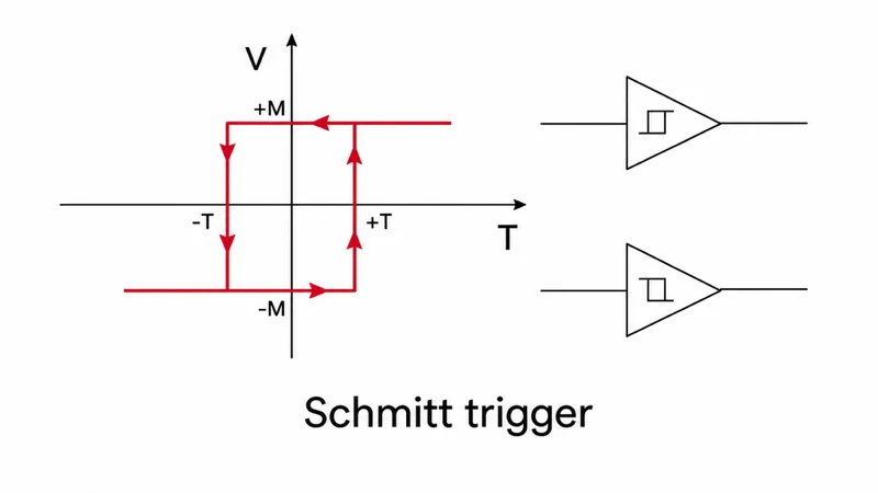
Schmitt trigger with positive feedback and hysteresis.
Key Takeaways
A Schmitt trigger is a comparator with positive feedback that uses separate upper and lower threshold voltages. The output switches when a rising input crosses the upper threshold and when a falling input crosses the lower threshold.
The difference between these trigger points is the hysteresis voltage, which provides noise immunity by preventing small input fluctuations from repeatedly switching the output.
In an inverting Schmitt trigger using an op-amp or comparator, the hysteresis width is determined by the feedback-network resistor ratio and output-voltage swing:
ΔV_H = (V_OH - V_OL) × R1/(R1 + R2)Schmitt trigger devices can have substantially different threshold and hysteresis specifications. For example, a 74HC14 can exhibit a typical hysteresis of about 0.98 V at 4.5 V, whereas the CD40106B's hysteresis varies considerably with supply voltage, temperature, and device characteristics.
A circuit exhibiting “Schmitt trigger action” is not necessarily a dedicated Schmitt-trigger input. For predictable interface design, check the datasheet for specified upper and lower threshold voltages (VT+ and VT−), hysteresis, input transition behavior, and operating conditions rather than assuming a generic logic input provides equivalent performance.
Introduction
A slowly changing or noisy input can cross a conventional logic threshold multiple times, causing unwanted transitions instead of a single clean digital edge. A Schmitt trigger solves this problem by using two switching thresholds rather than one. The separation between the upper and lower thresholds, known as hysteresis, prevents small voltage fluctuations from repeatedly changing the output state.
The circuit achieves this behavior through positive feedback. As the input rises, the output changes state when the input crosses the upper threshold voltage (VT+). As the input falls, the output switches back only after crossing the lower threshold voltage (VT−). The hysteresis width is therefore:
ΔV_H = VT+ - VT−
This simple change in threshold behavior makes the Schmitt trigger useful for signal conditioning, switch debouncing, waveform shaping, and converting slow or noisy analog signals into reliable digital transitions.
The concept originated with Otto Schmitt's work on electronic circuits for reproducing the switching behavior observed in biological systems. His early thermionic trigger established the principle that remains fundamental to modern implementations: positive feedback creates distinct switching conditions for rising and falling inputs.
Modern Schmitt trigger devices can be built using transistors, CMOS logic gates, comparators, or an op-amp. Although their circuits differ, they all use positive feedback to create two different threshold voltages: one for a rising input and another for a falling input. The difference between these thresholds creates hysteresis, which helps the circuit ignore small amounts of noise and produce a clean, stable output.
What Is a Schmitt Trigger Circuit?
A Schmitt trigger is a comparator circuit with positive feedback that uses different switching thresholds for rising and falling input signals. Instead of changing state whenever the input crosses one fixed threshold voltage, the circuit has an upper threshold voltage (VT+) for a rising input and a lower threshold voltage (VT−) for a falling input. Between these two levels, the output remains unchanged. This hysteresis gives the circuit a switching behavior that is resistant to small fluctuations and noise around the threshold.
The key mechanism is positive feedback. A portion of the output voltage is fed back to the input through a resistor network, changing the effective reference level according to the current output state. When the input crosses the active threshold, the output changes state; the feedback then shifts the threshold in the opposite direction, moving it farther away from the input voltage. This creates a deliberate separation between the two trigger points and prevents the output from immediately switching back because of a small input disturbance.
This behavior can be implemented with a comparator, an op-amp, or a transistor network. In a non-inverting Schmitt trigger, the input is applied to the non-inverting input while positive feedback establishes the switching thresholds. An inverting configuration reverses the relationship between input polarity and output state. Dedicated Schmitt trigger devices, such as CMOS logic gates, incorporate this hysteresis internally rather than requiring an external feedback network.
Recommended reading: Inverting vs Non-Inverting Op Amp: Complete Design Guide & Best Practices 2025
The Hysteresis Curve and Transfer Characteristics
The switching behavior becomes clearer when output voltage is plotted against input voltage. For a conventional single-threshold comparator, the output changes state at approximately one input level. A Schmitt trigger produces a different transfer characteristic because the switching point depends on whether the input voltage is increasing or decreasing.
The resulting hysteresis curve has two distinct transition points. A rising input must reach VT+ before the output changes state, while a falling input must drop below VT− before the output changes back. The voltage interval between these points is the hysteresis width:
ΔV_H = VT+ - VT−
Parameter | Symbol | Meaning |
Upper threshold voltage | VT+ | Input voltage at which the output switches when the input is rising |
Lower threshold voltage | VT− | Input voltage at which the output switches when the input is falling |
Hysteresis voltage | ΔV_H | Difference between the upper and lower thresholds |
The region between VT− and VT+ is often called the hysteresis band. While the input remains inside this band, the output does not change state solely because of the input voltage. This is the source of the Schmitt trigger's noise immunity: a noisy input can fluctuate within the hysteresis band without generating repeated output transitions.
For a practical logic device, however, the typical hysteresis curve is not enough to determine reliable system-level operation. Datasheets specify minimum and maximum threshold values over defined operating conditions. For example, Texas Instruments defines separate limits for positive-going and negative-going input transitions and specifies a region in which the device is guaranteed not to change state.
This distinction is important when designing an interface. A circuit should be designed around the worst-case threshold voltage, not the typical value shown in a transfer curve. The input signal must reach the specified positive-going threshold with adequate margin when switching high and fall below the negative-going threshold with adequate margin when switching low. Otherwise, variations in supply voltage, temperature, process, or noise can cause unreliable switching even when the nominal signal appears adequate.
Why Hysteresis Beats a Plain Comparator
A conventional comparator has a single switching threshold. When the input crosses that threshold, the output changes state. With a clean, fast-changing signal, this works well. However, a noisy input signal or a slow ramp can cross the threshold repeatedly, producing multiple output transitions when only one is expected.
The problem becomes more serious when a slow input remains near the switching threshold. As Texas Instruments explains, the output transition can briefly change the device's supply current and disturb the internal supply voltage. That disturbance can shift the effective switching threshold, causing the input to cross it again and trigger another transition. The resulting feedback can produce oscillation, excessive switching activity, and increased power consumption.
A Schmitt trigger breaks this cycle by introducing hysteresis. Instead of responding to one threshold, it uses separate upper and lower threshold voltages. Once the output changes state, the switching threshold moves away from the input, so small voltage fluctuations cannot immediately reverse the transition.
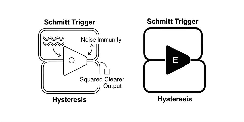
The size of the hysteresis band determines how much disturbance the circuit can tolerate. If the input noise remains within the hysteresis band, it cannot cause another transition. Toshiba similarly describes this behavior for CMOS Schmitt trigger devices, where noise or input bounce must exceed the specified hysteresis before it can produce an additional output transition.
For a first-order design, the hysteresis should therefore be greater than the expected peak-to-peak disturbance around the switching point:
ΔV_H > V_NOISE,PP
However, this is only a starting point. The designer must also consider the minimum signal amplitude that must be detected, threshold-voltage tolerance, supply variation, temperature, propagation delay, and the noise characteristics of the complete signal path. Excessive hysteresis can improve noise immunity but may also prevent the circuit from responding to legitimate small-amplitude signals.
Recommended reading: Why JFETS are Key in Low Noise Sensor Amplification
Schmitt Trigger Using Op-Amp: Inverting and Non-Inverting Designs
A Schmitt trigger using an op-amp or comparator uses positive feedback to create two switching thresholds. The resistor network determines the threshold voltage, while the output voltage swing determines the amount of hysteresis. The two basic configurations are the inverting and non-inverting Schmitt triggers. Their resistor arrangements and switching behavior are different, so their equations should not be interchanged.
Inverting Schmitt Trigger
In an inverting Schmitt trigger, the input signal is connected to the inverting terminal. The non-inverting input receives a voltage determined by the output through a feedback network and, when required, an external reference voltage, Vref.
For the topology in which R1 connects the output to the non-inverting input, and R2 connects that node to Vref, the switching thresholds are:
VT+ = Vref + (VOH - Vref) × R1/(R1 + R2)
VT− = Vref + (VOL - Vref) × R1/(R1 + R2)
The hysteresis width is:
ΔV_H = VT+ - VT−
ΔV_H = (VOH - VOL) × R1/(R1 + R2)
Here, VOH and VOL are the actual high- and low-level output voltages. They should not automatically be assumed to equal the supply rails, particularly when the op-amp does not have rail-to-rail output swing.
Worked example: Consider a 5 V supply, Vref = 2.5 V, VOH = 5 V, and VOL = 0 V. Let R1 = 10 kΩ and R2 = 100 kΩ. The feedback factor is:
β = R1/(R1 + R2)
β = 10/(10 + 100) = 0.0909
The upper threshold is:
VT+ = 2.5 + (5 - 2.5) × 0.0909 = 2.73 V
The lower threshold is:
VT− = 2.5 + (0 - 2.5) × 0.0909 = 2.27 V
Therefore:
ΔV_H = 2.73 - 2.27 = 0.46 V
or approximately 455 mV using the unrounded values.
Increasing R2 to 220 kΩ reduces the feedback factor:
β = 10/(10 + 220) = 0.0435
The resulting hysteresis is approximately:
ΔV_H = 5 × 0.0435 = 0.217 V
The thresholds become approximately 2.61 V and 2.39 V. In this configuration, the resistor ratio provides a direct way to trade noise immunity against switching sensitivity.
Non-Inverting Schmitt Trigger
A non-inverting Schmitt trigger uses a different topology. The input signal is connected to the non-inverting input through R1, while R2 provides positive feedback from the output to the same node. Vref is applied to the inverting terminal.
At the switching point, the voltage at the non-inverting input equals Vref. Applying Kirchhoff's current law at the input node gives:
(Vin - Vref)/R1 + (Vo - Vref)/R2 = 0
Solving for the input threshold voltage gives:
VT = Vref × (1 + R1/R2) - Vo × R1/R2
Because Vo can be either high or low, the threshold depends on the current output state. For a rising input, the output is initially low:
VT+ = Vref × (1 + R1/R2) - VOL × R1/R2
For a falling input, the output is initially high:
VT− = Vref × (1 + R1/R2) - VOH × R1/R2
The hysteresis width is therefore:
ΔV_H = (VOH - VOL) × R1/R2
Worked example: Using Vref = 2.5 V, R1 = 10 kΩ, R2 = 100 kΩ, VOH = 5 V, and VOL = 0 V:
VT+ = 2.5 × (1 + 10/100) - 0 × 10/100
VT+ = 2.75 V
For the falling transition:
VT− = 2.5 × (1 + 10/100) - 5 × 10/100
VT− = 2.25 V
Therefore:
ΔV_H = 2.75 - 2.25 = 0.50 V
The two configurations therefore have different resistor-to-hysteresis relationships. In the non-inverting topology, increasing R1 relative to R2 increases the hysteresis width. In the inverting topology described above, hysteresis is controlled by the divider fraction R1/(R1 + R2).
The input source also matters in the non-inverting configuration. Because the signal enters through R1, the source impedance effectively becomes part of the input resistance. If that impedance is significant compared with R1, it changes the effective resistor ratio and shifts the switching thresholds. The source impedance should therefore be included in the design calculations.
A Schmitt trigger using an op-amp is suitable for many low-frequency applications, but an op-amp is not optimized for open-loop switching. Its recovery from saturation, input common-mode range, output swing, slew rate, and propagation characteristics can limit switching performance. A dedicated comparator is generally the better choice when fast transitions, predictable propagation delay, and defined logic-level output behavior are required.
The Schmitt trigger should also not be confused with a conventional non-inverting amplifier. Although both circuits can use feedback around the non-inverting input, the feedback in a Schmitt trigger is deliberately regenerative. It creates two switching thresholds rather than establishing a fixed linear gain.
Inverting vs. Non-Inverting Schmitt Trigger
Feature | Inverting Schmitt Trigger | Non-Inverting Schmitt Trigger |
Input connection | Inverting terminal | Non-inverting input |
Feedback | Positive feedback to non-inverting input | Positive feedback to non-inverting input |
Reference | Non-inverting node | Inverting terminal |
Output response | Inverts input state | Follows input state |
Hysteresis equation | ΔV_H = (VOH - VOL) × R1/(R1 + R2) | ΔV_H = (VOH - VOL) × R1/R2 |
Main resistor relationship | Divider ratio | R1/R2 ratio |
Reference control | Convenient Vref adjustment | Vref sets the nominal decision level |
Typical advantage | Flexible threshold and hysteresis adjustment | Non-inverting signal response |
Recommended reading: Schmitt Trigger: Robust Comparator Design with Hysteresis
Transistor-Based Schmitt Trigger
A transistor-based Schmitt trigger can be built from two bipolar junction transistors (BJTs) arranged as an emitter-coupled pair. The transistors share a common emitter resistor, while the input is applied to the base of one transistor. The collector network provides the positive feedback that causes the circuit to switch rapidly between two stable states.
The circuit has two distinct operating states. When the input voltage is low, one transistor conducts while the other is largely off. As the input rises, the voltage at the input transistor's base eventually becomes high enough to overcome the base-emitter voltage and the voltage established at the shared emitter node. The input transistor then begins to conduct more strongly.
As its collector current increases, its collector voltage changes and drives the other transistor toward cutoff. This regenerative action rapidly transfers the current from one transistor to the other. The output therefore does not change gradually; instead, it makes a relatively fast transition between two states.
The shared emitter resistor plays an important role in establishing hysteresis. The emitter voltage depends on the current flowing through the conducting transistor pair. Because the current distribution differs between the two stable states, the shared emitter voltage also changes. Consequently, the input voltage required to switch the circuit in one direction is different from the voltage required to switch it back.
A simplified expression for the input switching condition is:
VT ≈ VE + VBE
where VT is the input threshold voltage, VE is the shared emitter voltage, and VBE is the transistor base-emitter voltage; it is the voltage difference between the transistor's base and emitter.
Because VE changes with the circuit's output state, the effective threshold also changes. The resulting separation between the two switching thresholds produces hysteresis:
ΔV_H = VT+ - VT−
This simplified relationship is useful for understanding the circuit, but it is not sufficient for precision design. The actual threshold voltages depend on transistor β, collector and emitter resistor values, load resistance, transistor saturation, supply voltage, and the operating currents of the devices. The commonly used 0.6–0.7 V approximation for VBE is also not a fixed value; it varies with collector current, temperature, and transistor characteristics. A practical design should therefore use the transistor's operating conditions rather than treating VBE as a constant.
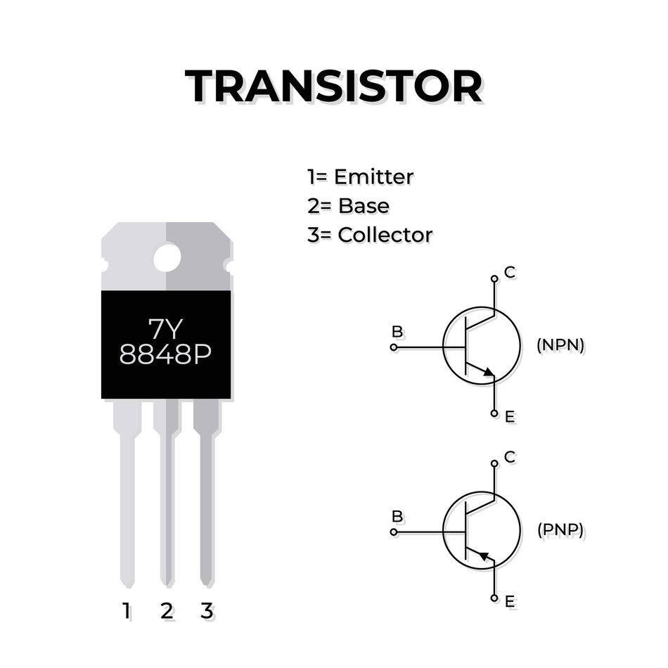
The main advantage of a transistor-based Schmitt trigger is flexibility. A designer can build the circuit from discrete components when a suitable integrated circuit is unavailable and can tailor its switching levels, output voltage, and drive characteristics to the application. Discrete implementations can also be useful when a required voltage range or switching behavior is not available from a standard logic device.
The same regenerative principle is used inside modern integrated Schmitt trigger devices, although the feedback network is implemented internally with transistors rather than discrete components. Understanding the discrete circuit therefore provides a useful physical picture of how positive feedback creates two stable states and separate trigger points.
Historically, other nonlinear devices, including the tunnel diode, were also used to produce bistable switching behavior through negative-resistance characteristics. Transistor and CMOS implementations became more practical for general-purpose signal conditioning and digital logic as semiconductor technology developed.
Feature | Transistor-Based Schmitt Trigger |
Core circuit | Two-transistor emitter-coupled pair |
Feedback mechanism | Regenerative positive feedback through the transistor network |
Switching states | One transistor conducts while the other is driven toward cutoff. |
Hysteresis source | State-dependent change in the shared emitter voltage |
Main threshold factors | VBE, emitter current, resistor values, transistor characteristics |
Advantages | Flexible, discrete, customizable |
Limitations | Device variation, temperature dependence, more design effort |
Typical applications | Signal conditioning, level detection, waveform shaping |
Recommended reading: NMOS and PMOS Transistors: Fundamentals and Applications
CMOS Schmitt Trigger Devices and Real Datasheet Numbers
Most modern designs use a packaged CMOS Schmitt trigger rather than building the hysteresis network from discrete components. These devices integrate the switching circuitry into a logic gate, providing defined threshold voltages, hysteresis, propagation delay, and output characteristics in a compact package. Common examples include the 74HC14, 74HCT14, and CD40106B, all of which provide multiple Schmitt trigger inverter channels in a single integrated circuit.
The familiar 74HC14 and related devices are Schmitt trigger inverters: a rising input eventually drives the output low, while a falling input drives the output high. Non-inverting Schmitt trigger devices are also available, although their part numbers vary by manufacturer and logic family. Designers should therefore verify the actual device function and threshold specifications in the datasheet rather than relying on the part-number suffix alone.

Comparing Real Parts
Threshold specifications can vary significantly between logic families and even between manufacturers using the same basic logic designation. The values below illustrate why the typical hysteresis value should not be used as the sole basis for a design.
Device | Supply | VT+ (min / typ / max) | VT− (min / typ / max) | Hysteresis (min / typ / max) |
SN74HC14 | 4.5 V | 1.55 / 2.5 / 3.13 V | 0.9 / 1.6 / 2.45 V | 0.4 / 0.9 / 2.1 V |
74HC14 (Nexperia) | 4.5 V | 1.7 / 2.38 / 3.15 V | 0.9 / 1.4 / 2.0 V | 0.4 / 0.98 / 1.4 V |
74HCT14 (Nexperia) | 4.5 V | 1.2 / 1.41 / 1.9 V | 0.5 / 0.85 / 1.2 V | 0.4 / 0.56 / n.s. |
CD40106B | 5 V | 2.2 / n.s. / 3.6 V | 0.9 / n.s. / 2.8 V | 0.3 / n.s. / 1.6 V |
CD40106B | 15 V | 6.8 / n.s. / 10.8 V | 4.0 / n.s. / 7.4 V | 1.6 / n.s. / 5.0 V |
n.s. = not specified.
Several important engineering conclusions follow from these specifications.
Guaranteed hysteresis can be substantially smaller than the typical value. For example, the Nexperia 74HC14 specifies a typical hysteresis of 0.98 V at 4.5 V, but the minimum specified hysteresis is only 0.4 V. A design that requires a particular level of noise immunity should therefore use the minimum guaranteed value rather than the typical value.
The switching thresholds are not necessarily centered around the supply voltage. For the Nexperia 74HC14 at 4.5 V, the typical positive-going threshold is 2.38 V, and the negative-going threshold is 1.4 V. The midpoint of these two thresholds is approximately 1.89 V, which is below half the supply voltage. This matters when the device is used to detect a signal whose expected transition level is assumed to be centered around mid-supply.
Supply voltage can substantially change the switching behavior. The CD40106B operates over a wide supply range, and its specified threshold voltages and hysteresis increase as the supply voltage increases. At 5 V, its specified hysteresis range is 0.3–1.6 V, compared with 1.6–5.0 V at 15 V. This makes high-voltage CMOS Schmitt trigger devices useful when a relatively large hysteresis band is required without adding an external feedback network.
Speed is another important difference between logic families. For example, the SN74HC14 has a typical propagation delay of about 12 ns at 4.5 V under the specified test conditions, while the CD40106B is considerably slower, with a typical propagation delay of approximately 140 ns at 5 V and 60 ns at 15 V. These values demonstrate why threshold specifications alone are not enough when selecting a Schmitt trigger for a timing- or frequency-sensitive application.
The actual datasheet conditions also matter. Threshold voltage, hysteresis, propagation delay, and output drive can depend on supply voltage, temperature, load capacitance, and other operating conditions. For a production design, use the manufacturer's guaranteed minimum and maximum specifications under the expected operating conditions rather than values taken from a typical transfer curve.
How CMOS Hysteresis Is Generated
A CMOS Schmitt trigger generates hysteresis internally through transistor-level positive feedback. Unlike an external op-amp or comparator circuit, it does not require a resistor network to establish separate switching thresholds. Instead, the relative sizing and arrangement of the internal MOSFETs determine how the circuit responds to rising and falling input voltages.
A simplified way to understand the operation is to consider the transistor network as changing the effective switching condition according to the current output state. When the input rises, the circuit reaches one threshold and changes state. That change alters the internal feedback currents, so the threshold for switching back is different. The result is the same fundamental behavior seen in a discrete Schmitt trigger:
ΔV_H = VT+ - VT−
At the transistor level, the threshold voltages depend on device parameters and transistor sizing. A commonly used MOSFET parameter is:
k = 0.5 × μCox × (W/L)
where μ is carrier mobility, Cox is the gate-oxide capacitance per unit area, and W/L is the transistor width-to-length ratio. Changing the relative sizing of the internal transistors changes their drive strengths and therefore changes the switching thresholds.
This approach gives semiconductor manufacturers control over the hysteresis characteristics during the integrated-circuit design process. However, it also means the user generally cannot externally adjust the hysteresis of a standard CMOS Schmitt trigger. If a design requires a precisely adjustable threshold or hysteresis band, an external comparator or op-amp circuit may be more appropriate.
For most digital signal-conditioning applications, however, the fixed hysteresis of a CMOS Schmitt trigger is an advantage. The manufacturer characterizes the switching thresholds, the feedback network requires no external components, and the device can directly produce a logic-compatible output. This makes CMOS Schmitt trigger devices particularly useful for signal conditioning, switch debouncing, waveform shaping, and converting slow or noisy signals into clean digital transitions.
Recommended reading: Voltage Regulator Design and Selection: Linear vs Switching, LDOs, and Practical Considerations
Building a Schmitt Trigger with a 555 Timer
The 555 timer contains the basic elements needed to create a Schmitt trigger: an internal voltage divider and two comparators with different reference levels. By connecting the trigger and threshold pins and using them as a single input, the 555 can operate as a Schmitt trigger with an inverting output.
For the standard bipolar 555 configuration, the internal voltage divider establishes nominal reference levels at approximately one-third and two-thirds of the supply voltage. At VCC = 5 V, these levels are approximately:
VT− ≈ VCC/3 ≈ 1.67 V
VT+ ≈ 2VCC/3 ≈ 3.33 V
At VCC = 15 V:
VT− ≈ 15/3 = 5 V
VT+ ≈ 2 × 15/3 = 10 V
The resulting hysteresis is therefore approximately:
ΔV_H = VT+ - VT−
ΔV_H = 2VCC/3 - VCC/3
ΔV_H = VCC/3
At a 5 V supply, this gives:
ΔV_H ≈ 5/3 ≈ 1.67 V
This is substantially wider than the hysteresis of many standard CMOS Schmitt trigger inputs. A large hysteresis band can be useful when the input signal contains significant noise or slow voltage variations because the signal must move through a relatively large voltage range before the output changes state again.
The trade-off is that a 555 timer is generally less attractive than a dedicated CMOS Schmitt trigger when low power, high switching speed, or compact digital interfacing is important. The bipolar NE555, for example, has significantly higher supply-current requirements than a CMOS logic device such as the 74HC14. Its switching performance is also strongly dependent on the particular 555 implementation and operating conditions. Designers should therefore compare propagation delay, rise and fall time, supply current, output drive, and operating voltage rather than comparing hysteresis alone.
The 555's control-voltage pin provides additional flexibility. In the standard configuration, the control-voltage input is connected to the internal reference network associated with the two-thirds-of-VCC threshold. Applying an external voltage to this pin can shift the comparator reference levels and therefore move the switching thresholds. This can be useful when the default one-third and two-thirds VCC thresholds do not match the required input signal levels.
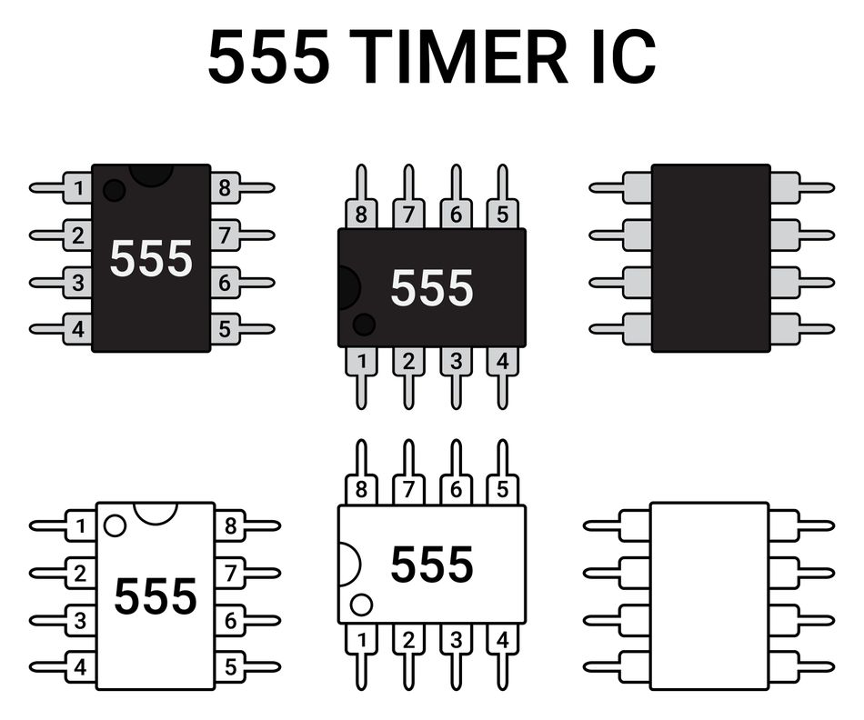
However, the control-voltage input should not be treated as an independent adjustment of the upper and lower thresholds. The two comparator references are related through the internal divider and comparator architecture, so changing the control voltage shifts the threshold conditions according to the 555's internal circuit. The manufacturer's datasheet should be used when calculating the resulting trigger and threshold levels.
The 555 approach is therefore most useful when a large, supply-scaled hysteresis band is desirable, and the additional power consumption and slower switching characteristics are acceptable. For low-power digital signal conditioning, a dedicated CMOS Schmitt trigger is usually the more efficient solution; for adjustable thresholds, an external comparator or op-amp Schmitt trigger provides greater control.
Applications
The value of a Schmitt trigger becomes most apparent when a real signal is imperfect. From mechanical switch bounce to noisy sensor outputs and simple oscillators, hysteresis allows the circuit to turn uncertain voltage changes into controlled, repeatable transitions.
Switch Debouncing
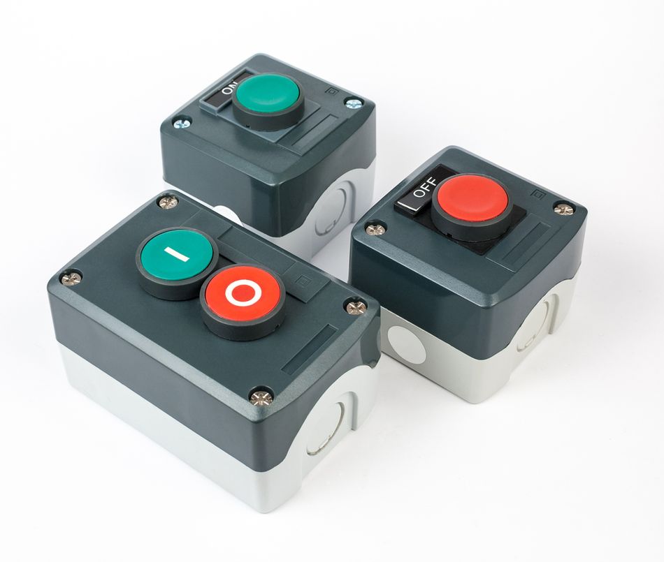
Mechanical switches can produce multiple rapid transitions, or contact bounce, when they open or close. The bouncing may last for milliseconds and can cause a digital input to register several transitions instead of one.
An RC network can filter the bounce by slowing the voltage change at the input, but the resulting waveform may still spend a significant amount of time near the logic threshold. A conventional gate with a single switching threshold can therefore respond to small fluctuations in the filtered signal and produce multiple output transitions.
A Schmitt trigger solves this problem by combining the RC filter with hysteresis. The capacitor smooths the bouncing waveform, while the separated upper and lower thresholds prevent small fluctuations from repeatedly changing the output state. Once the input crosses the active threshold, it must move through the hysteresis band before the output can switch back.
The RC time constant should be selected in relation to the expected bounce duration and the required response time. Making the time constant too large improves filtering but increases the delay before a legitimate switch is recognized. TI documents the use of a Schmitt trigger inverter for switch debouncing as a standard application.
Signal Conditioning and Sine-to-Square-Wave Conversion
A Schmitt trigger can convert a slowly varying or noisy analog waveform into a digital-like square wave. When a sine wave is applied to the input, the output changes state as the waveform crosses the upper and lower switching thresholds. Because the thresholds are separated, small amounts of noise around either crossing point are less likely to produce unwanted transitions.
For a periodic sine wave that crosses both thresholds once during each cycle, the output frequency remains equal to the input frequency. However, the output duty cycle depends on the positions of the switching thresholds relative to the waveform. If the positive-going and negative-going thresholds are not symmetrically positioned around the sine wave's midpoint, the high and low portions of the output will have different durations.
This makes the circuit useful for recovering digital timing signals from sensor outputs, tachometer signals, slowly changing waveforms, or signals that have degraded while traveling through a long cable. The Schmitt trigger provides signal conditioning by converting the uncertain analog transition into a well-defined logic transition.
For example, if a sine wave is centered at 0 V and the switching thresholds are symmetric at +VT and -VT, the resulting square wave can approach a 50% duty cycle. If the thresholds are offset from the waveform's center, the crossing times change and the duty cycle shifts accordingly.
Relaxation Oscillators
A Schmitt trigger can also be used with a resistor and capacitor to create a relaxation oscillator. In this configuration, the capacitor voltage continuously moves between the two switching thresholds. When the capacitor voltage reaches one threshold, the Schmitt trigger changes state, reversing the direction in which the capacitor charges or discharges.
For an inverting Schmitt trigger, the basic sequence is:
The output switches to the high state.
The capacitor charges toward the high output voltage.
The capacitor voltage reaches VT+.
The output switches to the low state.
The capacitor discharges toward the low output voltage.
The capacitor voltage reaches VT−.
The cycle repeats.
The oscillation frequency depends primarily on the resistor, capacitor, output voltage levels, and switching thresholds. Because practical Schmitt trigger devices have threshold tolerances, the actual oscillator frequency can vary from the nominal value.
This makes a Schmitt-trigger relaxation oscillator useful for simple timing and waveform-generation applications where high-frequency accuracy is not required. TI documents this type of oscillator using the 555 timer and Schmitt trigger circuits, while Nexperia also provides a relaxation-oscillator application for the 74HC14.
For applications requiring a precise frequency, however, a crystal oscillator, timer with a precision reference, or dedicated clock generator is generally more appropriate.
Level Detection and Set-Point Control
Schmitt triggers are also useful when a system must switch an output at a defined set point without repeatedly turning on and off near that point. This is common in thermostats, battery monitoring, fan controllers, level detectors, and other control systems.
Without hysteresis, a noisy measurement that fluctuates around the switching threshold can cause an actuator to chatter. For example, a temperature controller without sufficient hysteresis might repeatedly turn a fan on and off as the measured temperature moves slightly above and below the set point.
Adding hysteresis creates separate turn-on and turn-off conditions. The controlled variable must rise above one threshold to activate the output and fall below another threshold before the output deactivates. This prevents small measurement fluctuations from causing unnecessary switching.
The required hysteresis should be large enough to exceed the expected measurement noise and should also account for the dynamics of the controlled system. If the hysteresis is too small, the actuator may still chatter. If it is unnecessarily large, the controlled variable may move farther from the desired set point before the system responds.
This principle has a direct connection to the historical use of Schmitt-trigger circuits for thermostatic control. The same fundamental idea remains relevant in modern control systems: separate the activation and deactivation thresholds so that noise and small fluctuations do not cause repeated switching.
Design Considerations and Common Mistakes
A Schmitt trigger can make an unreliable input much more robust, but hysteresis does not eliminate every limitation of the circuit. Threshold tolerances, slow input transitions, source impedance, power consumption, and device selection all affect whether the design will behave as intended. The following mistakes are particularly common.
Confusing Schmitt-Trigger Action with a True Schmitt Trigger
Not every logic device that provides some hysteresis should automatically be treated as a Schmitt trigger. Some logic families incorporate a small amount of hysteresis to improve noise immunity while still specifying limits on input rise and fall time. A dedicated Schmitt trigger input, by contrast, is specifically characterized for operation with slowly changing input signals and provides defined positive-going and negative-going switching thresholds.
The distinction must be verified from the datasheet. Look for specifications such as VT+, VT−, or input hysteresis (ΔV_H). If the datasheet does not provide the threshold specifications or does not characterize the device for slow input transitions, do not assume that a small amount of internal hysteresis makes it suitable for the application.
Assuming Slow Inputs Are Free
Hysteresis prevents repeated switching caused by a slow or noisy input, but it does not necessarily eliminate the power penalty associated with a slow transition. In a CMOS input stage, an input voltage between the logic-low and logic-high regions can cause both the pull-up and pull-down transistor networks to conduct simultaneously. This produces additional supply current, often specified by manufacturers as ΔICC.
The additional power associated with slow input transitions can be significant when the input changes frequently. A commonly used expression is:
Padd = fi × (tr × ΔICC(AV) + tf × ΔICC(AV)) × VCC
where Padd is the additional power dissipation, fi is the input frequency, tr and tf are the input rise and fall times, ΔICC(AV) is the average additional supply current during the transition, and VCC is the supply voltage.
The practical implication is important: a Schmitt trigger can tolerate slow edges without repeatedly switching, but slow edges can still increase power consumption. The effect becomes more significant as input frequency, rise/fall time, or supply voltage increases.
Designing to Typical Thresholds
Typical threshold values are useful for understanding how a device normally behaves, but they are not design guarantees. Manufacturing variation, supply voltage, temperature, and device characteristics can shift the actual switching thresholds.
A robust design should therefore use the manufacturer's guaranteed minimum and maximum values. For hysteresis, use the minimum guaranteed hysteresis when determining the amount of noise the circuit can tolerate:
ΔV_H(min) = VT+(min) - VT−(max)
The exact relationship between the specified limits depends on how the manufacturer defines the parameters, so the datasheet's definitions should always take precedence.
Similarly, verify that the expected input signal crosses the guaranteed switching thresholds with sufficient margin rather than designing around the typical values shown on a hysteresis curve.
Using Too Much Hysteresis
Increasing hysteresis improves resistance to noise, but more hysteresis is not always better. The input must travel through a larger voltage range before the output can switch back, which can delay the response or prevent a small legitimate signal from reaching the opposite threshold.
The hysteresis band should therefore be large enough to reject the expected noise but small enough to accommodate the minimum valid signal excursion:
Vsignal, excursion > ΔV_H
This is a design trade-off rather than a rule that simply favors maximum hysteresis. The optimum value depends on the signal amplitude, noise level, required response time, and threshold tolerances.
Ignoring Source Impedance
Source impedance can alter the switching thresholds, particularly in a non-inverting Schmitt trigger where the input resistor forms part of the threshold-setting network. If the signal source has significant or variable output impedance, that impedance effectively becomes part of the circuit and can change the resistor ratios used in the threshold calculation.
For example, if the source resistance is comparable to the external input resistor, the effective resistance seen by the Schmitt trigger is different from the value assumed during the initial calculation. This can shift both trigger points and change the hysteresis.
The solution is to include the source impedance in the threshold calculation or buffer the signal with a suitable amplifier before applying it to the Schmitt trigger.
Using an Op-Amp Where a Comparator Is More Appropriate
An op-amp can be used to build a Schmitt trigger, but it is not necessarily the best device for every switching application. An op-amp is primarily designed for linear closed-loop operation, whereas a comparator is optimized for detecting which of two input voltages is larger and producing a fast output transition.
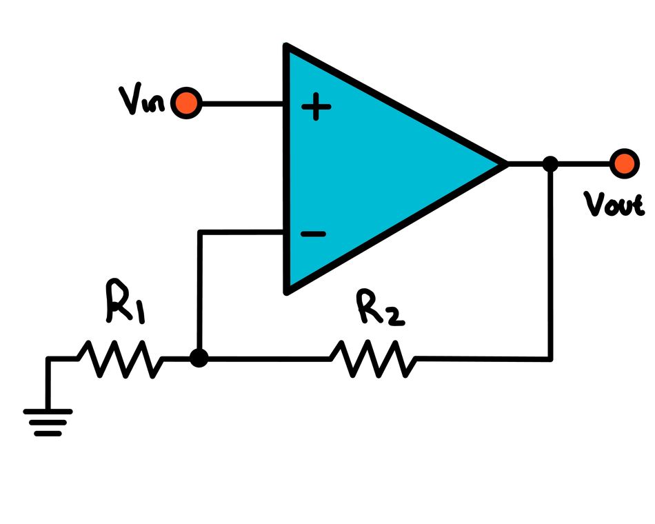
When an op-amp Schmitt trigger drives its output into saturation, recovery from saturation can introduce additional delay. The output may also have limited voltage swing, slew-rate limitations, and input common-mode constraints that affect the actual switching behavior.
For low-frequency signal conditioning, an op-amp can work well, particularly when adjustable thresholds or additional analog processing are required. For fast switching or timing-critical applications, a dedicated comparator with appropriate input and output specifications is generally the better choice.
Conclusion
A Schmitt trigger solves a fundamental signal-conditioning problem: it converts a slow, noisy, or ambiguous input near a decision point into a clean and decisive digital output. The key design task is determining where the upper and lower switching thresholds should be placed and how much hysteresis is required between them.
For many applications, a packaged Schmitt trigger inverter such as the 74HC14 or CD40106B is the simplest solution. The choice depends on the required hysteresis, switching speed, supply voltage, power consumption, and guaranteed threshold specifications. When the switching thresholds need to be customized, a comparator or op-amp Schmitt trigger provides greater control through the resistor network. For the inverting configuration discussed earlier:
ΔV_H = (VOH - VOL) × R1/(R1 + R2)
A 555 timer provides another option when a large, supply-scaled hysteresis band is useful. With its standard internal reference levels, the nominal hysteresis is approximately:
ΔV_H ≈ VCC/3
This can provide substantially more noise margin than many CMOS logic inputs, although the trade-offs include higher power consumption and slower switching.
Reliable Schmitt trigger design comes down to balancing noise immunity, signal amplitude, switching speed, and threshold tolerance. Size the hysteresis using the worst-case noise and minimum valid signal, then verify the design against the manufacturer's guaranteed threshold and hysteresis limits rather than relying on typical datasheet values.
Frequently Asked Questions
What is the main purpose of a Schmitt trigger circuit?
A Schmitt trigger converts a slow, noisy, or uncertain input into a clean digital output. It uses separate upper and lower switching thresholds so that small voltage fluctuations within the hysteresis band do not cause unwanted output transitions.
What is the difference between a comparator and a Schmitt trigger?
A conventional comparator typically uses a single switching threshold. A Schmitt trigger adds positive feedback to create separate thresholds for rising and falling input signals. This hysteresis helps prevent repeated switching when the input is noisy or remains close to the switching point.
How do you calculate the hysteresis of a Schmitt trigger using an op-amp?
The hysteresis depends on the specific circuit topology and resistor network. For the inverting configuration described in this guide, it is determined by the output voltage swing and the feedback-divider ratio. A non-inverting configuration uses a different resistor relationship, so the equations should not be interchanged.
How much hysteresis does a 74HC14 have?
At 4.5 V, the Nexperia 74HC14 specifies a hysteresis voltage of 0.4 V minimum, 0.98 V typical, and 1.4 V maximum. Its typical positive-going threshold is 2.38 V, while its typical negative-going threshold is 1.4 V. Actual values vary with operating conditions and should be checked against the datasheet limits.
Can a 555 timer be used as a Schmitt trigger?
Yes. Connecting the threshold and trigger pins allows a 555 timer to operate as an inverting Schmitt trigger. In the standard configuration, the switching levels are approximately two-thirds and one-third of the supply voltage. With a 5 V supply, these correspond to approximately 3.33 V and 1.67 V.
Why does my Schmitt trigger output still oscillate?
First, verify that the device is a true Schmitt trigger with specified upper and lower switching thresholds. Some logic devices provide limited hysteresis or “Schmitt trigger action” while still having restrictions on input rise and fall times. Also check whether the input noise exceeds the device's guaranteed minimum hysteresis. Designing from typical hysteresis values can leave insufficient noise margin under worst-case conditions.
What is the difference between an inverting and non-inverting Schmitt trigger?
An inverting Schmitt trigger produces an output that changes in the opposite direction to the input, while a non-inverting Schmitt trigger produces an output that follows the input. Both use positive feedback to establish separate switching thresholds, but their circuit topologies and threshold equations are different.
Who invented the Schmitt trigger?
The Schmitt trigger is named after Otto H. Schmitt, who developed the circuit while studying nerve impulse propagation. He described the thermionic trigger in his 1938 paper, A Thermionic Trigger.
References
[1] Texas Instruments, “Understanding Schmitt Triggers,” Application Brief SCEA046. [Online]. Available: https://www.ti.com/document-viewer/lit/html/scea046
[2] Nexperia, “74HC14; 74HCT14: Hex inverting Schmitt trigger,” Datasheet, Feb. 2024. [Online]. Available: https://www.nexperia.com/products/analog-logic-ics/logic/buffers-inverters-transceivers/inverters/serie/74hc14-74hct14
[3] O. H. Schmitt, “A thermionic trigger,” Journal of Scientific Instruments, vol. 15, no. 1, pp. 24–26, 1938.
[4] I. M. Filanovsky and H. Baltes, “CMOS Schmitt trigger design,” IEEE Transactions on Circuits and Systems I: Fundamental Theory and Applications, vol. 41, no. 1, pp. 46–49, Jan. 1994, doi: 10.1109/81.260219.
[5] Texas Instruments, “TLC555 CMOS Timer,” Datasheet. [Online]. Available: https://www.ti.com/product/TLC555
[6] Analog Devices, “Activity: The Comparator, Positive Feedback and Schmitt Trigger, for ADALM1000,” Analog Devices Wiki. [Online]. Available: https://wiki.analog.com/university/courses/alm1k/alm-lab-comp
[7] Georgia State University, “Schmitt Trigger,” HyperPhysics. [Online]. Available: https://hyperphysics.gsu.edu/hbase/Electronic/schmitt.htm
in this article
1. Key Takeaways2. Introduction3. What Is a Schmitt Trigger Circuit?4. The Hysteresis Curve and Transfer Characteristics5. Why Hysteresis Beats a Plain Comparator6. Schmitt Trigger Using Op-Amp: Inverting and Non-Inverting Designs7. Transistor-Based Schmitt Trigger8. CMOS Schmitt Trigger Devices and Real Datasheet Numbers9. Building a Schmitt Trigger with a 555 Timer10. Applications11. Design Considerations and Common Mistakes12. Conclusion13. Frequently Asked Questions14. References