RF Design Methodology: From Specification to Verification
A guide covering the full radio-frequency design workflow, starting from setting specifications and choosing topologies to matching, simulation, layout, and verification, to help antenna engineers.

26 May, 2026. 13 minutes read
Key Takeaways
Radio-frequency design is a multi-staged process that defines requirements, builds a link budget and architecture, selects component topologies, simulates, optimizes, and implements the layout with controlled impedance.
Specification parameters such as frequency band, bandwidth, output power, noise figure, linearity (IIP3), error vector magnitude (EVM), and adjacent channel power ratio (ACPR) set quantitative targets.
Parasitic inductance, capacitance, and resistance cause discrete components to become reactive at high frequencies. The self-resonant frequency (SRF) defines the usable range; above the SRF, inductors behave capacitively, and capacitors behave inductively.
Lumped L-, T- and Pi-networks provide conjugate matches at a single frequency, while distributed microstrip stubs and quarter-wave transformers are used at higher frequencies. The choice balances bandwidth (Q), component count and ease of tuning.
Circuit-level tools (Keysight ADS, Cadence AWR/Microwave Office) handle linear and nonlinear simulations; 3D electromagnetic solvers (ANSYS HFSS, Sonnet) analyze field distributions and PCB structures.
Introduction
Wireless systems are present everywhere, ranging from smartphones and Wi-Fi 7 access points to 77 GHz automotive radars and sub-GHz IoT sensors. Achieving reliable, regulatory-compliant performance in these systems hinges on robust radio-frequency (RF) design. Unlike digital circuits, RF design operates in regions where the wavelength may be comparable to component dimensions and interconnect lengths; parasitics dominate the behavior, and impedance matching becomes critical. Whereas printed circuit board (PCB) fabrication focuses on process control and manufacturing tolerances, RF design encompasses specification, topology selection, matching networks, simulation, layout, and measurement.
This article provides an engineering-oriented workflow for RF design, emphasizing both theoretical principles and practical implementation across frequency ranges from HF through millimeter-wave. It differentiates itself from fabrication-focused guides by addressing the complete design lifecycle and by providing quantitative guidance with examples grounded in standards such as Wi-Fi 6E/7, 5G NR, Bluetooth, GPS and automotive radar.
What Is RF Design?
Radio-frequency design relates to circuits and systems operating between a few megahertz and the lower millimetre-wave range. The most commonly used standard reference impedance is 50 Ω because it provides a compromise between power handling and low attenuation in coaxial cables.
The minimum attenuation occurs near 77 Ω while maximum power handling occurs near 30 Ω, and 50 Ω lies between these extremes. RF frequencies are typically categorised as:
Band | Frequency range | Examples |
HF to VHF | 3 MHz – 300 MHz | Sub-GHz IoT, FM radio, VHF data links |
UHF and L-band | 300 MHz – 1 GHz | ISM bands (315 MHz, 433 MHz), GPS (1.575 GHz) |
S-band and C-band | 1 GHz – 6 GHz | Wi-Fi 4/5/6 (2.4 GHz, 5 GHz), Bluetooth, Wi-Fi 6E (6 GHz) |
X-band and Ku-band | 6 GHz – 18 GHz | Radar altimeters, satellite communications |
mmWave (Ka, V, W) | 24 GHz – 110 GHz | 5G FR2 (n258 24.25–27.5 GHz, n257 26.5–29.5 GHz, n260 37–40 GHz), automotive radar 77–81 GHz |
At low frequencies where the wavelength is much greater than circuit dimensions, lumped components behave ideally, and the designer can assume a uniform current distribution.
But when frequencies approach the gigahertz range, trace lengths become a significant fraction of the wavelength, component parasitics emerge, and distributed effects dominate. The 50 Ω reference line enables predictable matching and measurement using vector network analyzers.
Suggested Reading: Why is Picking the Right Trace Width Important?
RF Design Workflow
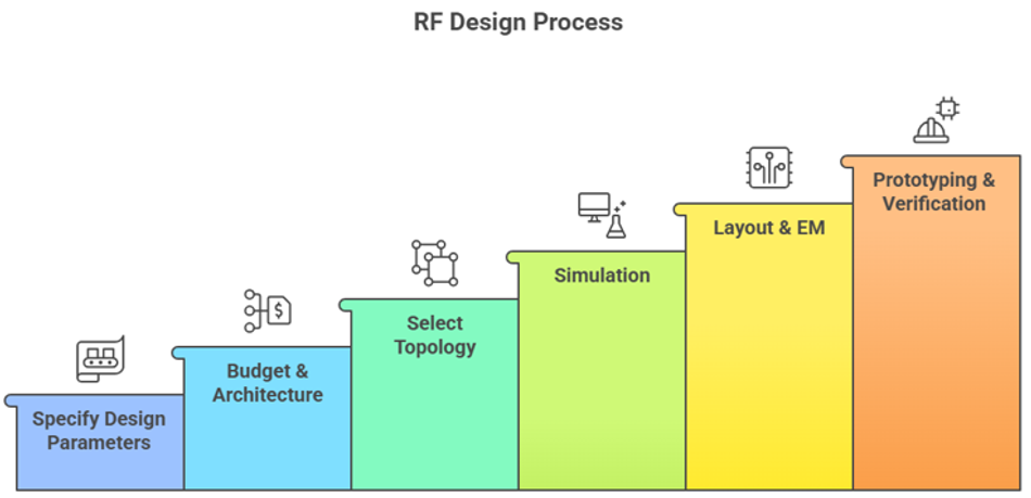
A disciplined RF design process minimizes iterations while ensuring that performance targets are met. In this section, we will discuss the key stages of an RF design process.
Specifying Design Parameters
The first step is to define the specifications for your RF design. The main objective is to set quantitative goals for various design parameters, such as frequency band, bandwidth, modulation, transmit power, sensitivity, noise figure, linearity (IIP3), EVM, ACPR, and power consumption.
Moreover, designers focus on environmental and regulatory constraints like FCC Part 15, ETSI EN 300 328, 3GPP TS 38, and IEEE 802.11.
Budget & Architecture Linking
This step is perhaps the most critical of all, as designers pick the target components based on the design specifications. In this phase, it is a common practice to calculate path loss, which is calculated using the following formula:

Where the length d is in km, while f is in MHz.
Moreover, designers specify gains, antenna losses, receiver sensitivity, and transmitter power, and determine the transceiver architecture, such as a superheterodyne or a direct-conversion block diagram.
Selecting Topology and Schematics
At this stage, designers pick suitable circuit topologies. These topologies must be carefully selected to ensure minimal noise and maximum efficiency.
Typically, designers look for low-noise amplifiers, oscillators, mixers, filters, and power amplifiers. In this phase, the gain, noise figure, compression points, and IIP3 parameters are chosen from datasheets.
Simulation
The selected design parameters and schematics are then tested via simulation. With highly advanced simulation tools and electromagnetic solvers, designers evaluate the RF design performance virtually.
Moreover, designers use linear S-parameter analysis and harmonic-balance simulation (in ADS or AWR) to assess gain, stability, and impedance matching. HFSS and Sonnet are two useful tools for verifying transmission lines and antenna structures.
Suggested Reading: The Fundamentals of RF Testing and Measurement Techniques
Layout & Layout Level EM
After virtual testing, the finalized designs are forwarded for transformation into a physical design. Various parameters, such as microstrip, stripline, and coplanar waveguides, are considered at this stage. Moreover, designers pick suitable substrate materials and stackup.
Usually, planar EM simulators such as Momentum or AXIEM are used to model coupling and resonances and to adjust trace width and length.
Prototyping and Verification
This is the last stage of the design phase. The verified virtual design undergoes fabrication. This step is pretty similar to a PCB fabrication process and includes component installation, calibration, etc.
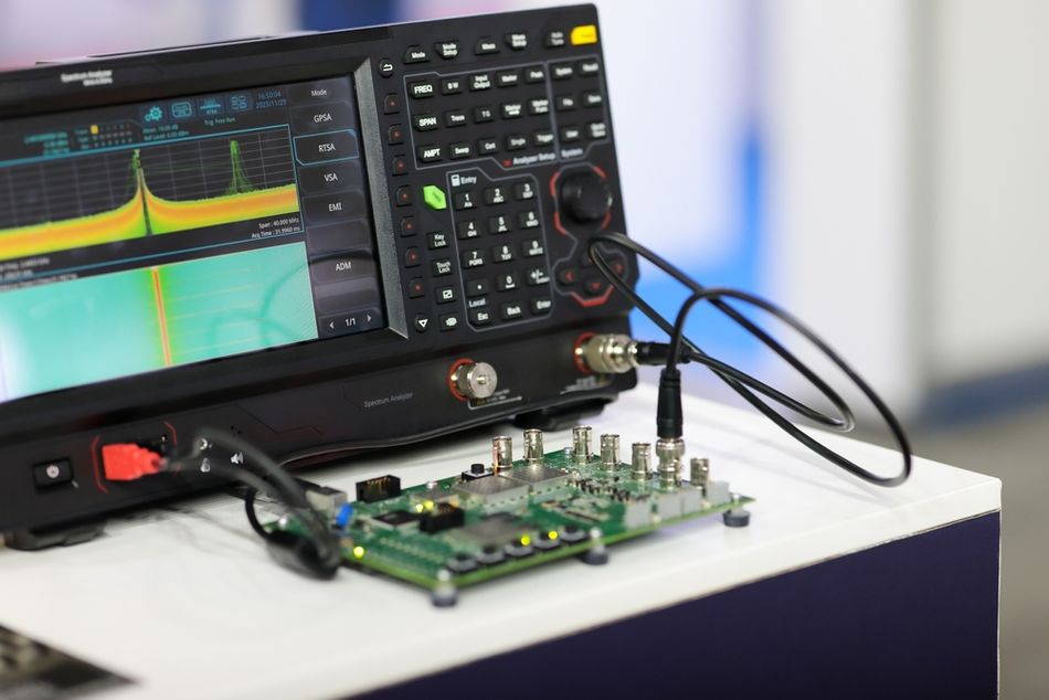
Designers typically use vector analyzers and spectrum analyzers to measure S-parameters and power and spectral emissions, respectively. Moreover, a time-domain reflectometer (TDR) is used to measure impedance discontinuities.
Suggested Reading: RF PCB: Design, Materials, and Manufacturing Processes
Specifications and Link Budgets
RF design begins with a clear understanding of the parameters that define system performance:
Parameter | Description | Example / Notes |
Operating Frequency & Bandwidth | Determines antenna size, component behavior, and regulatory constraints. | Wi-Fi 7 operates at 2.4 GHz, 5 GHz, and 5.925–7.125 GHz (6 GHz band). 5G NR divides frequencies into FR1 (410 MHz–7.125 GHz) and FR2 (24.25–52.6 GHz). |
Transmit Power | Regulatory standards define the maximum allowed radiated power. | ETSI EN 300 328 limits 2.4 GHz devices to 20 dBm EIRP. |
Receiver Sensitivity | The minimum input signal level required for an acceptable signal-to-noise ratio (SNR). | A GPS receiver may require sensitivity as low as -130 dBm. |
Noise Figure (NF) | Measures how much the RF circuit degrades the signal-to-noise ratio. | Typical LNAs have NFs of 0.9–2.3 dB, while mixers may have NFs around 13 dB. NF is calculated using: NF(dB)=10 log10(F) |
Linearity (IIP3) | Indicates the circuit’s tolerance to in-band distortion and intermodulation effects. | High-linearity VGAs such as the Analog Devices MAX2062 achieve output IP3 of +41 dBm. Input IP3 equals output IP3 minus gain. |
Compression Point (P1dB) | The input or output power level where gain compresses by 1 dB. | Power amplifiers must maintain the required output power without excessive distortion near the compression point. |
Error Vector Magnitude (EVM) & ACPR | Measure modulation accuracy and adjacent channel leakage. | Required for compliance with standards such as 3GPP TS 38 and IEEE 802.11. |
Recommended Reading: How to Specify an RF Antenna: RF Antenna Operation, Design, Selection, Testing, & Verification
How Do Components Behave at RF?
At low frequenies, electronic components tend to behave well within the set limits required for normal operation. .But As the frequencies get higher, the behavior needs critical overseeing. Here are some key aspects of component behavior at RF.
Parasitics and Self-resonance
Discrete resistors, capacitors, and inductors are prone to parasitic inductance, capacitance, and resistance that dominate at high frequencies.
Inductors have distributed inter-winding capacitance. Above the self-resonant frequency (SRF), the inductive reactance becomes capacitive.
Capacitors similarly have parasitic inductance and series resistance; at their series resonant frequency, the capacitive reactance cancels the inductive reactance, leaving only the equivalent series resistance (ESR). Above this frequency, the capacitor behaves inductively.
Resistors exhibit parasitic inductance from leads and a frequency-dependent resistance due to skin effect.
Skin Effect and Conductor Loss
At RF, current is confined to the surface of conductors within one skin depth δ = √(ρ/πfμ). The conduction at one skin depth is 36.8 % of the DC value, and adding thickness beyond five skin depths yields a negligible reduction in RF resistance. It means that copper thickness above ~100 µm provides little benefit above several gigahertz.
Transmission Lines
When the trace length approaches λ/10, distributed transmission-line models are required. Commonly, microstrip, stripline, and coplanar waveguide (CPW) are used.
For 50 Ω microstrip on FR-4 (εr ≈ 4.4), the trace width is approximately 1.9 × the dielectric height; 0.031-inch (0.79 mm) FR-4 requires ~59 mil (1.5 mm) width, and 0.062-inch (1.57 mm) FR-4 requires ~118 mil (3 mm).
FR-4 is practical to nearly 6 GHz. Beyond that, dielectric loss causes ~0.5 dB/inch insertion loss at 5 GHz and dielectric constant variation causes ±5 % impedance tolerance.
Stripline traces, surrounded by dielectric on both sides, require narrower widths (~12 mil) for 50 Ω. Low-loss substrates such as Rogers RO4350B (Dk = 3.48 ± 0.05, loss tangent impedance= 0.0037 at 10 GHz) offer improved performance at microwave frequencies.
Impedance Matching
Matching networks transform the complex impedance of a source or load to a standard reference impedance, usually 50 Ω, to maximise power transfer and minimise reflections. The selected topology depends on bandwidth, component quality factor (Q), and application requirements.
An L-network uses one series and one shunt reactive element. It is simple, low-loss, and suitable for narrowband impedance matching such as antenna-to-amplifier connections.
T-networks use two series and one shunt element, providing greater flexibility and moderate bandwidth for amplifiers and filters.
Pi-networks contain two shunt and one series element, offering broader impedance transformation and suitability for high-power amplifier stages.
Quarter-wave transformers use λ/4 transmission-line sections for wideband matching at higher frequencies.
For narrowband systems, L- or Pi-networks are often sufficient, whereas broadband designs may require T-networks or multi-section transformers. The Smith chart is widely used to visualize impedance matching.
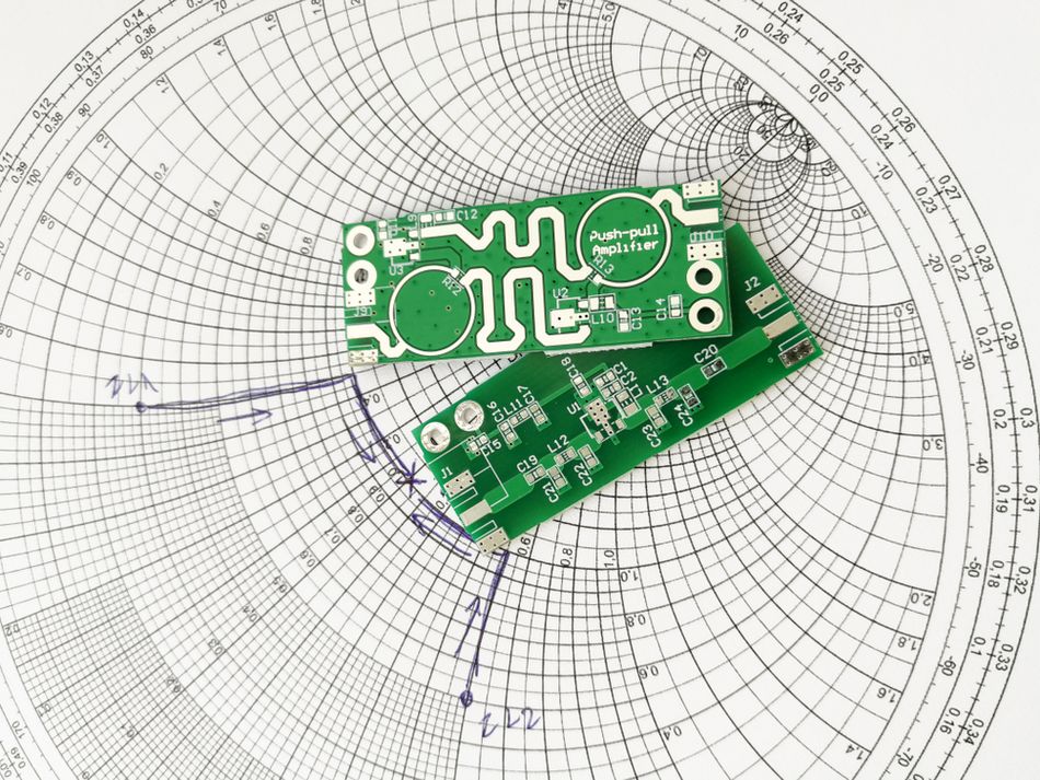
Matching networks transform the complex impedance of a source or load to a standard reference impedance, usually 50 Ω, to maximize power transfer and minimize reflections.
Suggested Reading: Controlled Impedance: A Comprehensive Guide
Filters and Amplifiers
Filter responses
Three classical responses dominate RF filter design:
Butterworth: Maximally flat pass-band amplitude response (no ripple) but the slowest roll-off. Suitable for test equipment and precision measurement.
Chebyshev Type I: Introduces an equiripple pass-band to achieve a steeper transition; typical ripple 0.1–0.5 dB. A 5th-order elliptic filter with 0.1 dB ripple achieves 50 dB rejection at 1.3× the cutoff; a Chebyshev requires a 7th-order filter, and a Butterworth a 10th-order filter to match the same rejection.
Elliptic (Cauer): Allows ripple in both pass-band and stop-band, giving the steepest possible roll-off for a given order. Suitable when size and component count must be minimized and some ripple can be tolerated.
Chebyshev filters are widely used in receiver preselectors because the moderate ripple is manageable.
Recommended Reading: Low Pass Filter vs High Pass Filter – Theory, Design, and Applications
Low-Noise Amplifiers (LNAs)
LNAs set the noise figure and linearity of the receiver front end.
Typical LNAs provide 10–20 dB gain with noise figures as low as 0.9 dB (MAX2640) and 2.3 dB (MAX2645 high-gain).
The relationship between output IP3 and input IP3 is IIP3 = OIP3 – gain; high-linearity devices (OIP3 ≈ +41 dBm) are available.
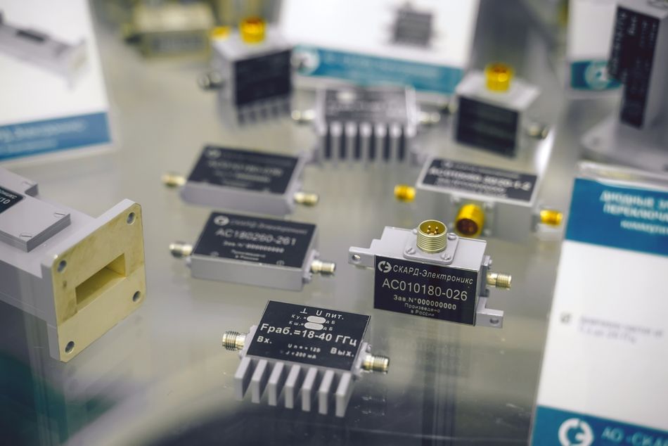
LNAs often use inductive degeneration and feedback to achieve stability and match the input impedance. When designing LNAs, ensure stability across the operating bandwidth (Rollet's stability factor K > 1) and include ESD protection and bias networks.
Suggested Reading: Difference between Active and Passive Filters?
PCB Layout for RF
Controlled-impedance traces
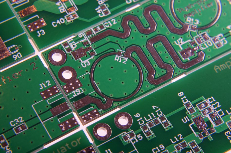
Controlled-impedance traces use microstrip or stripline calculations to achieve target impedance values. On FR-4, a 50 Ω microstrip requires wider traces than stripline due to dielectric placement. PCB stack-up, copper thickness, and impedance tolerance should be specified to the fabricator.
Ground Planes and Shielding
Ground planes minimize loop area and parasitic inductance, while stitching vias and via fences suppress resonances and isolate circuit sections. Decoupling capacitors should be placed close to supply pins with multiple capacitance values for broadband filtering.
Thermal Considerations
Thermal design is essential for power amplifiers, requiring thermal vias and copper spreading areas. Sensitive analog circuits should be isolated from high-power and digital sections to minimize interference.
Suggested Reading: Thermal Management in PCB Design: Meeting Standards for Heat Dissipation
Simulation and EDA Tools
Selecting the right tool accelerates design and reduces errors. The following table summarizes the common simulation tools.
Tool | Type | Strengths | Typical applications |
Keysight ADS (PathWave ADS) | Circuit/system simulator with integrated planar EM (Momentum) | Linear S-parameter, harmonic balance and circuit envelope simulations; integrated schematic, layout and design kits; includes Momentum planar EM and optional FEM 3D simulation. | RF circuit design (LNAs, mixers, PAs), filter synthesis, system-level design and co-simulation. |
Cadence AWR/Microwave Office | Circuit and system design platform with AXIEM and Analyst EM solvers | Provides schematic capture, optimisation, and design synthesis; AXIEM is a 3D planar method-of-moments solver for planar structures; advanced meshing yields efficient simulation. | Filters, matching networks, phased-array antenna feed networks, circuit-EM co-simulation. |
ANSYS HFSS | Full-wave 3D electromagnetic finite element solver | High accuracy for complex 3D structures like antennas, waveguides and connectors; adaptive meshing and multi-physics capabilities. | Antenna design, packaging, 3D waveguide components, electromagnetic compatibility analysis. |
Sonnet Suites | Shielded-domain method-of-moments planar EM solver | Delivers model extraction error on the order of 1 % for 3D planar circuits; accurately analyses microstrip, stripline, filters and spiral inductors. | High-precision modelling of planar structures on stratified substrates; integrated with Microwave Office via EM Socket interface. |
Qucs / QucsStudio | Open-source circuit simulator | Supports S-parameter, transient and harmonic balance analyses; good for educational use and quick feasibility studies. | Entry-level RF circuit design and teaching. |
Measurement and Verification
Accurate RF measurement requires calibration and error correction to obtain reliable S-parameter results from vector network analyzers (VNAs). Measurement errors are commonly classified as:
Systematic errors – leakage, mismatch, and frequency-response effects
Random errors – noise and connector repeatability
Drift errors – temperature-related variations
Calibration methods such as SOLT and TRL use known standards (open, short, load, through) to minimise these errors. Two-port calibration uses 12 error terms to improve accuracy.
Fixture parasitics from coaxial-to-microstrip transitions are removed using de-embedding, allowing measurements to represent the actual device. Modern VNAs support real-time de-embedding for interactive tuning.
Standards and Compliance
Regulatory compliance ensures the coexistence of wireless devices and limits interference. Key standards include:
FCC Part 15: Governs unlicensed devices in the United States, specifying radiated and conducted emission limits and prohibiting harmful interference.
ETSI EN 300 328: Harmonized standard for wideband transmission systems in the 2.4 GHz band. For non-adaptive frequency-hopping equipment, the maximum RF output power is capped at 20 dBm EIRP, and duty cycle, dwell time, and hopping requirements govern spectrum usage.
3GPP TS 38 series: Defines physical layer requirements for 5G NR, including frequency ranges (FR1 and FR2), channel bandwidths, modulation formats (up to 256-QAM), and performance metrics (EVM, ACPR).
IEEE 802.11 (Wi-Fi): Specifies wireless LAN protocols. Wi-Fi 7 (802.11be) operates in the 2.4 GHz, 5 GHz, and 6 GHz bands with channel widths up to 320 MHz, 4096-QAM modulation, and multi-link operation.
MIL-STD-461/810: Military standards for electromagnetic compatibility and environmental testing (vibration, shock, temperature). Designs for aerospace and defense must meet these rigorous requirements.
Compliance testing often involves accredited laboratories and certification bodies. Designers should factor regulatory limits into specifications early to avoid costly redesigns.
Suggested Reading: Mastering PCB Testing: Techniques, Methods, and Best Practices Unveiled
Conclusion
RF design is a multidisciplinary engineering practice that balances theory and practical constraints. A methodical workflow — starting with clear specifications and link budgets, choosing appropriate topologies, simulating and optimizing, implementing a controlled-impedance layout, and measuring with calibrated instruments — minimizes risk and accelerates development. Quantitative parameters such as noise figure, IIP3, P1dB, return loss, and group delay guide decisions at each stage.
The balance between efficiency and linearity in power amplifiers, the parasitic effects in high-frequency components, and the challenges of millimeter-wave propagation are the key aspects needed for a deep understanding. Looking ahead, trends such as AI-assisted design, integrated mmWave RFICs, beamforming arrays, and terahertz systems promise both opportunities and challenges. By mastering the fundamentals and embracing new tools and techniques, RF, hardware, mixed-signal, and antenna engineers can deliver robust, high-performance wireless systems across the spectrum.
FAQ
1. What is RF design?
Radio-frequency design is used to create circuits and systems that operate at frequencies where wavelengths are comparable to component dimensions. It’s a study of specification, link budgeting, matching networks, simulation, layout and verification, ensuring that amplifiers, filters, antennas and transmission lines work together to meet performance and regulatory requirements.
2. Why is 50 Ω the standard impedance in RF systems?
The 50 Ω reference offers a compromise between minimum loss (which occurs near 77 Ω) and maximum power handling (near 30 Ω) in coaxial cables. Using a standard impedance simplifies component design, matching, and measurement because instruments such as network analyzers and filters are specified for 50 Ω.
3. How do I match impedance in RF circuits?
Use matching networks to transform source or load impedances to the reference impedance. Lumped L-networks provide narrowband matching with two components; T- and Pi-networks offer more bandwidth at the cost of additional elements. Also, there are distributed techniques like quarter-wave transformers and stub tuners, which are used at higher frequencies.
4. Which simulation tool should I use for RF design?
Choose based on the level of abstraction. Keysight ADS and Cadence AWR/Microwave Office are well-suited for circuit- and system-level simulation, with integrated planar EM solvers. ANSYS HFSS provides high-accuracy 3D field simulation for antennas and complex packaging. Sonnet Suites offers very accurate planar EM analysis for microstrip and stripline circuits with model extraction error around 1 %.
5. What is noise figure and why does it matter?
Noise figure (NF) quantifies how much a circuit degrades the signal-to-noise ratio (SNR). It is defined as NF = 10·log₁₀(F), where F is the noise factor (ratio of output SNR to input SNR). Low NF is critical in receivers because any noise added by the first amplification stage is amplified by subsequent stages. A high noise figure directly reduces receiver sensitivity.
6. What's the difference between RF design and RF PCB design?
RF design encompasses the entire workflow from specification through verification, including system architecture, link budget, component selection, matching, simulation and measurement. RF PCB design focuses specifically on the physical implementation of the circuit — selecting substrates, controlling trace impedance, managing grounding and shielding, and meeting fabrication tolerances.
7. How do I lay out RF PCB ground planes?
Use continuous ground planes adjacent to signal layers to provide a return path and minimise inductive loops. Stitch ground vias along microstrip edges at intervals no longer than λ/10 to maintain a low-impedance enclosure. Place decoupling capacitors close to device power pins and route signals orthogonally between layers to reduce coupling.
8. Why are Chebyshev and elliptic filters popular in RF design?
Chebyshev filters achieve steeper roll-off than Butterworth filters by allowing equiripple pass-band response with typical ripple 0.1–0.5 dB. Elliptic filters place transmission zeros in both pass-band and stop-band to provide the sharpest transition; a 5th-order elliptic filter with 0.1 dB ripple can achieve 50 dB rejection at 1.3 × the cutoff frequency, while lower-order Chebyshev or Butterworth filters cannot.
References
Cadence System Analysis. "Inductor Parasitic Capacitance Limits Upper Operating Frequencies." https://resources.system-analysis.cadence.com/blog/inductor-parasitic-capacitance-limits-upper-operating-frequencies
Johanson Technology. "SRF and PRF for RF Capacitors." https://www.johansontechnology.com/tech-notes/srf-prf-for-rf-capacitors/
FlowCAD. "Cadence AWR AXIEM 3D Planar EM Simulator." https://www.flowcad.com/en/awr-axiem.htm
Microwave Journal. "AWR Connected for Sonnet: EM-Socket II Integration in NI AWR Design Environment." https://www.microwavejournal.com/articles/27800-awr-connected-for-sonnet-now-supports-em-socket-ii-architecture-within-v13-ni-awr-design-environment
IIT Madras MEMS. "Error Corrections: VNA Calibration Tutorial." https://mems.iitm.ac.in/eservice/sites/default/files/charactrazation_file/Error_Corrections-VNA.pdf
5G Technology World. "How Doherty Amplifiers Improve PA Efficiency." https://www.5gtechnologyworld.com/how-doherty-amplifiers-improve-pa-efficiency/
Microwaves101. "Why Fifty Ohms?" Encyclopedia entry. https://www.microwaves101.com/encyclopedias/why-fifty-ohms
Knowles Capacitors. "An Introduction to the 5G Frequency Spectrum." https://blog.knowlescapacitors.com/blog/an-introduction-to-the-5g-frequency-spectrum
ETSI. "EN 300 328 V2.2.2: Wideband Transmission Systems Operating in the 2.4 GHz Band." https://www.etsi.org/deliver/etsi_en/300300_300399/300328/02.02.02_60/en_300328v020202p.pdf
Analog Devices (Maxim Integrated). "Noise Figure Measurement Methods and Formulas." https://www.analog.com/en/resources/technical-articles/noise-figure-measurement-methods-and-formulas--maxim-integrated.html
Analog Devices. "IP3 and Intermodulation Guide." https://www.analog.com/en/resources/technical-articles/ip3-and-intermodulation-guide.html
Cadence PCB Resources. "RF Sheet Resistance and Conductor Loss." https://resources.pcb.cadence.com/blog/2024-rf-sheet-resistance
RF Essentials. "Microstrip Trace Width for 50 Ω Impedance on FR-4." https://rfessentials.com/rf-knowledge-base/how-do-i-determine-the-correct-microstrip-trace-width-for-50-ohm-impedance-on-fr/
Rogers Corporation. "RO4350B Laminates Datasheet." https://www.rogerscorp.com/advanced-electronics-solutions/ro4000-series-laminates/ro4350b-laminates
RF Essentials. "Butterworth vs Chebyshev vs Elliptic Filter Responses." https://rfessentials.com/rf-knowledge-base/what-is-the-difference-between-butterworth-chebyshev-and-elliptic-filter-respons/
IIT Madras MEMS. "Embedding and De-embedding S-parameters: VNA Tutorial." https://mems.iitm.ac.in/eservice/sites/default/files/charactrazation_file/Embedding_and_De-embedding_S-parameters-VNA.pdf
Dynamic Engineers. "Differences Between EDA Software ADS and HFSS." https://www.dynamicengineers.com/content/differences-between-eda-software-ads-and-hfss
in this article
1. Key Takeaways2. Introduction3. What Is RF Design?4. RF Design Workflow5. Specifications and Link Budgets6. How Do Components Behave at RF?7. Filters and Amplifiers8. PCB Layout for RF9. Simulation and EDA Tools10. Measurement and Verification11. Standards and Compliance12. Conclusion13. FAQ14. References