VCXO Design Guide: Voltage-Controlled Crystal Oscillator
VCXO (voltage-controlled crystal oscillator) is a precision timing device that enables fine frequency control. This article explains how VCXOs work, their tuning range, Kv, key specifications, circuit design, applications, alternatives, and how to select the right device.

27 Aug, 2026. 40 minutes read
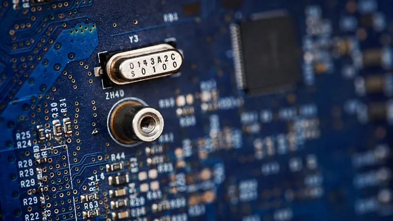
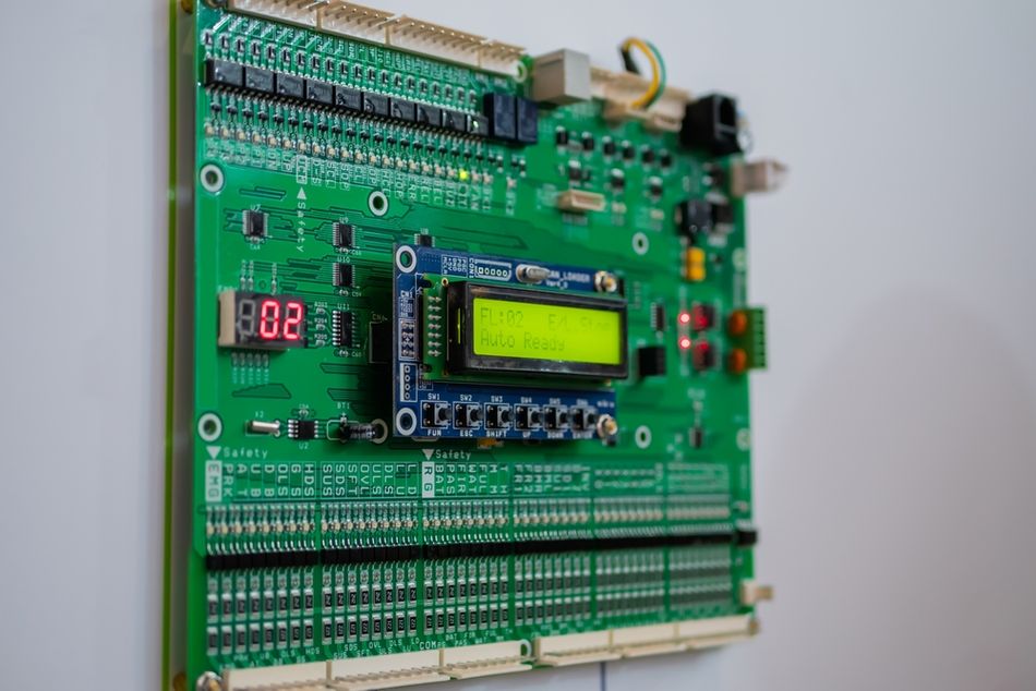
Quartz crystal oscillator on a printed circuit board
Key Takeaways
Varactor-based tuning: A VCXO uses a quartz crystal as its frequency-selective resonator and a voltage-variable capacitance, typically provided by a varactor diode, to adjust the effective load seen by the crystal. Changing the control voltage changes the capacitance and shifts the oscillation frequency.
Narrow but precise tuning: Quartz VCXOs typically provide a limited tuning range compared with conventional voltage-controlled oscillators (VCOs). Depending on the crystal, circuit, and specification, tuning may be specified in ppm relative to the nominal output frequency. The absolute pull range (APR) describes the total frequency adjustment available after accounting for factors such as initial tolerance, temperature, aging, and other frequency errors.
Tuning slope and linearity: The tuning sensitivity, commonly expressed as Kv in Hz/V or ppm/V, describes how much the oscillation frequency changes for a given change in control voltage. Linearity describes how closely this relationship follows the expected tuning curve across the specified voltage range. Both parameters affect loop design, especially in phase-locked loops (PLLs).
Pull range involves trade-offs: Increasing the electrical pull range generally requires a larger change in the crystal's effective load capacitance. This can increase sensitivity to circuit parasitics and may affect phase noise, frequency stability, and tuning linearity. Designers should therefore specify enough pull range to meet the system requirement without adding unnecessary tuning sensitivity.
Applications: VCXOs are used where a stable reference frequency must be adjusted electronically. Common applications include PLLs, clock generators, jitter attenuators, clock and data recovery, telecommunications, network synchronization, and precision audio and video timing. Output interfaces can include LVCMOS, LVDS, LVPECL, and HCSL, depending on the application.
Alternatives and complements: TCXOs and OCXOs provide stronger temperature stability when frequency accuracy is the primary concern, while VCOs offer much wider tuning ranges at the cost of generally higher phase noise. MEMS-based oscillators and digitally controlled architectures can provide other combinations of tuning range, programmability, stability, and ultra-low jitter. The appropriate choice depends on the required frequency range, stability, phase-noise or jitter performance, and control architecture.
Introduction
A VCXO (voltage-controlled crystal oscillator) is a precision oscillator that combines the frequency stability of a quartz crystal with electronic frequency control. Unlike a fixed-frequency crystal oscillator, a VCXO changes its output frequency in response to a control voltage. Its tuning range is relatively narrow, but the frequency resolution and stability can be useful in timing systems that must track an external reference. This makes the VCXO a common building block in phase-locked loops (PLLs), clock and data recovery, network synchronization, clock generators, and jitter attenuators.
The frequency-selective element in a VCXO is a high-Q quartz crystal resonator. The oscillator circuit adds a variable capacitance, commonly implemented with a varactor diode, to change the effective load capacitance presented to the crystal. As the control voltage changes, the varactor capacitance changes, shifting the crystal's load-dependent oscillation frequency. The resulting frequency deviation is usually specified in ppm, while the change in frequency per volt of control input is described by the tuning sensitivity, or Kv. The relationship between control voltage and frequency is not necessarily linear, so the specified tuning characteristic and linearity are important when the VCXO operates inside a PLL.
The key design challenge is to obtain enough frequency adjustment without sacrificing the properties that make quartz useful for precision timing. A wider pull range generally requires a larger change in the effective load capacitance and can make the oscillator more sensitive to parasitic capacitance, control-voltage noise, and nonlinearities in the crystal's load curve. The available pullability also depends on the crystal parameters, oscillator topology, and load-capacitance range.
This creates an important distinction between a VCXO and other crystal-based oscillators. A TCXO uses temperature compensation to improve frequency stability over temperature, while an OCXO maintains the crystal in a controlled-temperature environment to achieve still greater stability. Both can also be combined with voltage control to form TC/VCXO or OC/VCXO architectures.
For a VCXO, therefore, selecting the largest available tuning range is rarely the right design strategy. The required frequency deviation must be considered together with Kv, control-voltage range, tuning linearity, frequency stability, phase noise, jitter, temperature range, aging, and the requirements of the timing loop. In a network synchronization or jitter-attenuation application, the VCXO is part of a larger control system, so its electrical characteristics must be matched to the PLL bandwidth and loop dynamics rather than evaluated in isolation.
Principle of Operation and Circuit Architecture
A VCXO controls frequency by changing the electrical load presented to a quartz crystal. The sections below examine how load capacitance produces frequency pulling, how tuning range and Kv are specified, and how the control and output stages affect practical VCXO performance.
Load-capacitance pulling
A quartz crystal has both series and parallel resonance, and its operating frequency depends on how it is connected to the oscillator circuit. In a typical VCXO, the crystal operates close to its parallel-resonant region, where the external load capacitance affects the oscillation frequency. This capacitance includes the crystal's static capacitance, external capacitors, varactor capacitance, package capacitance, and PCB parasitics.
A practical crystal equivalent circuit consists of a motional branch containing resistance, inductance, and capacitance in parallel with the crystal's static capacitance, usually denoted as C0. The motional capacitance may be denoted as Cm or C1, depending on the notation used by the manufacturer. The series-resonant frequency is determined primarily by the motional inductance and capacitance, while the parallel-resonant frequency is also affected by the static and external load capacitance. Changing the capacitance connected to the crystal therefore changes its operating frequency. This effect is known as frequency pulling.
A common VCXO architecture uses a Pierce oscillator. The quartz crystal connects between the input and output of an inverting amplifier, while capacitive elements establish the load seen by the crystal. In a voltage-controlled implementation, a varactor diode is incorporated into this load network. The varactor is a reverse-biased PN junction whose capacitance changes with applied voltage.
The control voltage therefore changes the varactor capacitance rather than directly changing the mechanical resonance of the crystal. As the varactor capacitance changes, the effective load capacitance seen by the crystal changes, shifting the oscillator's frequency.
For a simplified crystal model, the approximate frequency-pulling relationship can be expressed as:
Δf ≈ fs × Cm / [2(C0 + CL)]
where:
Δf = approximate frequency shift
fs = crystal series-resonant frequency
Cm = motional capacitance
C0 = crystal static capacitance
CL = effective external load capacitance
This expression is an approximation. A practical VCXO calculation must account for the complete load network, including the varactor, fixed capacitors, oscillator input and output capacitance, package parasitics, and PCB stray capacitance.
The direction of the tuning response depends on the circuit configuration. In a common positive-slope implementation, increasing the control voltage reduces the varactor capacitance and increases the output frequency. However, designers should not assume this polarity from the term "VCXO" alone. The manufacturer should specify whether the device has a positive or negative tuning slope.
Recommended reading: Crystal Oscillator: Fundamentals, Models, and Design Guidelines
Typical pulling range and absolute pull range
A quartz VCXO has a much narrower tuning range than a conventional VCO because the quartz crystal constrains operation to a small frequency region around its nominal value. The usable tuning range is normally specified in ppm, Hz, or both. Pull ranges of tens to a few hundred ppm are common, but there is no universal value for all VCXOs. The achievable range depends on the crystal, operating frequency, load network, varactor characteristics, control-voltage range, and oscillator architecture.
Two related specifications are important when evaluating tuning capability: total pull range and absolute pull range (APR). Total pull range describes the frequency excursion available as the tuning voltage moves across its specified range. APR is more useful for system design because it represents the frequency correction that remains after other frequency errors consume part of the available tuning range.
A simplified relationship can be written as:
APR ≈ Total Pull Range - Frequency Tolerance - Temperature Stability - Aging
The exact calculation depends on the manufacturer's definitions and on which error terms are included. Renesas, for example, calculates APR by accounting for frequency tolerance, temperature stability, and aging when evaluating VCXO crystal selection.
For example, consider a VCXO with a total pull capability of ±113 ppm. If initial frequency tolerance, temperature-related deviation, and aging consume a combined ±55 ppm, approximately ±58 ppm remains as usable APR:
APR ≈ ±113 ppm - ±55 ppm
APR ≈ ±58 ppm
The example is simplified, but it illustrates why nominal pull range should not be confused with guaranteed correction capability.
This distinction is important in phase-locked loops (PLLs). The VCXO must have enough APR to compensate for the frequency difference between the local oscillator and the reference while remaining within its specified control-voltage range. Designing from total pull range alone can leave insufficient margin once manufacturing tolerance, temperature, aging, and other frequency errors are included.
Tuning sensitivity, Kv, and linearity
The tuning sensitivity, commonly represented by Kv, describes how much the oscillator frequency changes for a given change in control voltage. It may be specified in Hz/V or ppm/V.
For example, a sensitivity of 100 ppm/V means that a 1 V change in control voltage produces approximately 100 ppm of frequency change around the specified operating point. The equivalent sensitivity in Hz/V can be calculated from the nominal output frequency:
Kv(Hz/V) ≈ f0 × Kv(ppm/V) / 10^6
For a 100 MHz VCXO with a sensitivity of 100 ppm/V:
Kv ≈ 100 MHz × 100 ppm/V / 10^6
Kv ≈ 10 kHz/V
Kv is not necessarily constant across the complete control-voltage range. The varactor's capacitance-voltage characteristic is nonlinear, and the crystal's frequency response to changes in effective load capacitance is also nonlinear. As a result, the frequency-versus-voltage curve can deviate from a straight line.
Linearity describes how closely this frequency-versus-control-voltage characteristic follows the specified ideal or best-fit response. Poor linearity means that the incremental Kv changes with control voltage. This can complicate PLL modeling because the effective gain of the controlled oscillator is no longer constant across its tuning range.
A higher Kv reduces the control-voltage excursion needed to produce a given frequency correction. However, it also increases the conversion of control-node noise into frequency modulation. If the control voltage contains a small disturbance vn(t), the corresponding frequency disturbance can be approximated as:
Δf(t) ≈ Kv × vn(t)
when Kv is expressed in Hz/V.
This creates an important design trade-off. A high-Kv VCXO can provide greater frequency correction for a given control-voltage range, but it also becomes more sensitive to noise on the control input. A lower-Kv device generally requires a larger voltage excursion for the same correction. The appropriate Kv therefore depends on the required APR, control-voltage range, PLL architecture, and system jitter budget. For example, the Si595 provides selectable Kv values and recommends selecting the smallest value that meets the required APR.
Control-voltage range and input characteristics
The control-voltage range is a device-specific specification and should be considered separately from the supply-voltage range. A VCXO may operate from a 1.8 V, 2.5 V, 3.3 V, or other supply while using a defined analog control range that does not span the full supply voltage.
Manufacturers specify the minimum and maximum control voltages over which the tuning performance is guaranteed. Operating outside this range does not necessarily provide additional useful frequency adjustment. The varactor and tuning network may instead enter a region where additional control voltage produces progressively less frequency change.
The control input also has finite impedance and capacitance. These characteristics affect the design of the control circuit and any filtering connected to the input. More importantly, noise coupled onto the control node can be converted into frequency and phase modulation through Kv.
For a small control-voltage disturbance vn(t), the frequency disturbance can be approximated as:
Δf(t) ≈ Kv × vn(t)
This relationship explains why the control-voltage path deserves careful attention in low-jitter designs. Filtering, grounding, PCB routing, power-supply noise, and coupling from nearby digital signals can all affect the spectral purity of the control signal and, consequently, the oscillator output.
The required filter must also be compatible with the timing-loop dynamics. Excessive filtering can slow the control response, while insufficient filtering can allow unwanted noise to reach the VCXO. In a PLL, the control-path filter should therefore be designed together with the loop bandwidth rather than treated as an isolated RC network.
Modulation bandwidth
A VCXO does not respond instantaneously to changes in its control voltage. The control network, varactor, oscillator circuitry, and crystal dynamics determine how quickly the output frequency can follow a changing control signal.
Modulation bandwidth is therefore a dynamic characteristic that must be taken from the specific device's datasheet or characterized for the particular oscillator design. It should not be treated as a universal property of all quartz VCXOs.
This characteristic becomes important when the VCXO is used for frequency modulation or inside a PLL. The PLL determines how quickly the control voltage changes, while the VCXO must respond predictably over the frequency range relevant to the loop. If the VCXO introduces significant additional dynamics within the intended loop bandwidth, then those dynamics must be included in the loop-stability analysis.
A wider control bandwidth can enable faster frequency correction but can also expose the oscillator to a wider range of control-node noise. Conversely, a narrower response can provide greater filtering of high-frequency control disturbances but may limit how quickly the oscillator can track the reference.
Output stages and signal formats
The oscillator core produces a periodic waveform, but the signal available at the output pin depends on the output buffer. A VCXO can provide a sine wave, clipped-sine output, or a single-ended or differential digital waveform.
Common clock interfaces include LVCMOS (Low-Voltage Complementary Metal-Oxide-Semiconductor), LVDS (Low-Voltage Differential Signaling), LVPECL (Low-Voltage Positive Emitter-Coupled Logic), and HCSL (High-Speed Current-Steering Logic). These interfaces differ in voltage swing, common-mode voltage, termination requirements, power consumption, and signal-integrity characteristics. The output format should therefore be selected according to the receiving device and transmission path.
LVCMOS is a single-ended CMOS clock interface commonly used where the receiver is located close to the oscillator. It is simple to implement, but its relatively large voltage transitions can produce supply and substrate noise if the layout is not carefully controlled.
LVDS uses differential signaling with a relatively small voltage swing. It provides good common-mode noise rejection and is useful when the clock must travel across a controlled-impedance PCB trace or cable.
LVPECL is another differential clock interface. It uses a current-steering architecture and generally requires carefully designed termination and biasing. Its higher signal levels and fast transitions can provide good timing performance, but the interface can consume more power than lower-swing alternatives.
HCSL is a current-mode clock interface widely associated with PCI Express and related high-speed digital systems. Its termination and switching characteristics differ from those of both LVDS and LVPECL, so the receiver and routing requirements must be considered when selecting a VCXO output format.
The output stage also contributes to the overall jitter budget. A quartz oscillator may provide excellent intrinsic frequency stability and low phase noise, but the final clock can still show increased jitter because of output-buffer noise, supply disturbances, PCB coupling, electromagnetic interference, or receiver sensitivity.
For this reason, a VCXO should be evaluated as part of the complete clock path. The crystal, oscillator core, control input, output buffer, power supply, PCB, and receiving circuitry all contribute to the final timing performance.
Key Specifications and Trade-offs
A VCXO datasheet contains several specifications that must be evaluated together. Pull range, Kv, linearity, frequency stability, phase noise, jitter, control-voltage range, and aging all affect whether the oscillator can meet the timing requirements of the system. The most important specifications are summarized below.
Specification | What it means | Design implications |
Absolute Pull Range (APR) | The guaranteed frequency-correction range remains after specified frequency errors are accounted for. Values vary widely by device and application. | APR must be sufficient to accommodate the reference and local-oscillator frequency errors required by the PLL. A larger APR provides more tracking margin but should not be selected without considering noise and tuning sensitivity. |
Tuning sensitivity (Kv) | The change in oscillator frequency for a change in control voltage, usually specified in ppm/V or Hz/V. | Higher Kv provides more frequency correction per volt but also increases sensitivity to noise on the control-voltage input. |
Linearity | The deviation of the frequency-versus-control-voltage characteristic from a specified best-fit or ideal response. | Poor linearity causes the effective Kv to change across the tuning range and can complicate accurate PLL modeling and loop-gain calculations. |
Control-voltage range | The voltage range over which the manufacturer guarantees the specified tuning performance. | The control circuit must provide the required voltage range without exceeding the VCXO input limits. The usable range is device-specific and should not be assumed from the supply voltage. |
Modulation bandwidth | The dynamic response of the VCXO to changes in control voltage. | It determines how rapidly the oscillator can respond to frequency-control changes and can affect PLL loop-bandwidth selection and frequency-tracking behavior. |
Control-input impedance and capacitance | The electrical loading presented by the VCXO control input. | These parameters affect the control-loop filter, noise filtering, and interaction between the VCXO and the preceding control circuitry. |
Phase noise and jitter | Phase noise describes spectral phase fluctuations, while jitter describes timing variation over a defined integration bandwidth. | These specifications determine the oscillator's contribution to the system timing budget. They must be evaluated at the relevant offset frequencies and jitter-integration bandwidth. |
Frequency stability | The change in oscillator frequency caused by temperature, supply variation, load effects, aging, and other specified conditions. | Frequency errors consume part of the available tuning range. Stability specifications must therefore be considered when calculating APR. |
Aging | The gradual change in oscillator frequency over time. | Aging reduces the frequency margin available for tracking and should be included when calculating the required APR over the intended service life. |
Absolute Pull Range
Absolute pull range (APR) is one of the most important specifications when a VCXO operates inside a PLL. It represents the frequency-correction capability available after the oscillator's other specified frequency errors have been considered. These errors can include initial frequency tolerance, temperature stability, supply sensitivity, load sensitivity, and aging, depending on the manufacturer's definition.
A simplified relationship is:
APR ≈ Total Pull Range - Frequency Tolerance - Temperature Stability - Aging
The actual calculation should follow the manufacturer's specification because not every datasheet defines APR in exactly the same way.
APR must be large enough for the VCXO to compensate for the frequency error that the timing loop needs to correct. Renesas' VCXO guidance makes this point explicitly: if the VCXO does not have sufficient APR to cover the required reference-frequency variation, the PLL may lose lock at a frequency extreme.
APR can vary considerably between VCXO architectures and products. For example, Renesas lists programmable VCXO devices with APR values ranging from ±4.5 ppm to ±754.5 ppm. This illustrates why designers should select APR from the actual system error budget rather than relying on a generic VCXO value.
Tuning sensitivity and Kv
Kv describes the frequency change produced by a change in control voltage. It is commonly specified in ppm/V for crystal oscillators or Hz/V for oscillator and PLL calculations.
The conversion between the two forms is:
Kv(Hz/V) = f0 × Kv(ppm/V) / 10^6
where f0 is the nominal oscillator frequency.
For example, a 100 MHz VCXO with a Kv of 100 ppm/V has a tuning sensitivity of:
Kv = 100 MHz × 100 ppm/V / 10^6
Kv = 10 kHz/V
Kv is not necessarily constant across the complete control range because the varactor capacitance and crystal pulling characteristic are nonlinear. Datasheets may therefore specify a nominal Kv, a minimum and maximum value, or a programmable oscillator gain.
Modern programmable VCXOs can cover a much wider Kv range than a simple generic specification suggests. For example, the Renesas 8N3QV01 provides selectable oscillator gains from approximately 7.57 ppm/V to 477.27 ppm/V at 3.3 V, and from 10 ppm/V to 630 ppm/V at 2.5 V.
Higher Kv is not automatically better. If the control-voltage noise is vn, the resulting frequency disturbance can be approximated as:
Δf ≈ Kv × vn
A higher Kv therefore converts a given control-voltage disturbance into a larger frequency disturbance. Renesas specifically recommends using the lowest Kv that satisfies the application's requirements for improved phase-noise performance.
Linearity
Linearity describes how closely the frequency-versus-control-voltage characteristic follows a specified straight-line response. Manufacturers may define it as the maximum deviation from a best-straight-line fit over a specified control-voltage range.
Linearity matters because a nonlinear tuning curve means that the effective Kv changes with control voltage. A PLL designed using a single nominal oscillator gain may therefore behave differently at different points in the VCXO's tuning range.
For example, the Renesas 8N3QV01 specifies control-voltage linearity using best-straight-line-fit variation and specifies a typical value of ±0.1% over the defined control-voltage range.
For applications that require accurate frequency modulation or predictable PLL behavior, designers should therefore examine the complete tuning curve rather than relying only on the nominal Kv value.
Control-voltage range
The control-voltage range defines where the VCXO's specified tuning behavior is guaranteed. It should not be assumed that the control range is always 0 V to VDD or that the center frequency always occurs at VDD/2.
These characteristics are device-specific. For example, the Renesas 8N3QV01 specifies a control-voltage tuning range from 0 V to VCC and a nominal control voltage of VCC/2. Those values apply to that device and should not be generalized to every VCXO.
The control input also has finite impedance and capacitance. These characteristics affect the design of the external loop filter and noise-suppression network. A high-impedance control input can reduce loading, but the designer must still consider input capacitance, PCB leakage, coupled noise, and the impedance of the driving circuit.
Modulation bandwidth
Modulation bandwidth describes how rapidly the oscillator responds to changes in its control voltage. It is particularly important when a VCXO operates inside a PLL, because the oscillator must respond predictably over the frequency range covered by the loop.
This parameter is device-specific. For example, the Renesas 8N3QV01 specifies a 100 kHz modulation bandwidth. Other VCXO architectures can have substantially different dynamic characteristics.
A wider bandwidth can allow faster frequency correction and tracking, but it also allows more high-frequency control-path noise to influence the oscillator. The VCXO response should therefore be considered together with the PLL loop bandwidth, loop filter, reference noise, and desired jitter attenuation.
Phase noise and jitter
Phase noise and jitter describe related but different aspects of oscillator timing performance. Phase noise describes the spectral distribution of short-term phase fluctuations around the carrier, while jitter describes timing variation integrated over a specified frequency-offset range.
A VCXO's phase-noise performance depends on factors including the crystal resonator, oscillator circuit, output frequency, drive level, power-supply noise, and output buffer. The pull range also matters because the crystal and tuning network determine how strongly control-voltage disturbances are converted into frequency and phase modulation.
However, it is too broad to state that a larger APR automatically reduces crystal Q or increases phase noise. The relationship depends on the oscillator and crystal design. A better design rule is to select the smallest pull range and Kv that satisfy the required frequency-correction range while meeting the system's noise and jitter budget.
This approach is supported by practical VCXO products. Renesas, for example, recommends using the lowest Kv that meets the application's APR requirement to obtain better phase-noise performance.
Frequency stability and aging
Frequency stability describes how much the oscillator frequency changes under specified environmental and operating conditions. Temperature is often a major contributor, but supply voltage, load conditions, and aging can also affect the frequency.
These effects are important because every frequency error consumes part of the available pull range. A VCXO with a nominally large tuning range may have considerably less usable APR after temperature and aging are included.
Aging represents the gradual change in frequency over time. The relevant specification depends on the crystal cut, resonator construction, operating conditions, package, and required service life. Rather than assuming a universal value such as ±1 ppm/year, designers should use the aging specification provided for the selected device or crystal.
The central design trade-off
The central VCXO design trade-off is not simply “wider tuning range versus lower stability.” The more useful engineering relationship is between required frequency-correction capability, tuning sensitivity, control-node noise, linearity, and oscillator noise performance.
A wider pull range provides more frequency-correction margin, which can be valuable in a PLL that must accommodate large reference or oscillator errors. However, achieving that range can require a crystal and tuning network with greater electrical sensitivity. This can increase sensitivity to control-voltage noise, parasitic capacitance, component tolerances, and nonlinearities.
Similarly, a higher Kv allows the PLL to correct frequency with a smaller control-voltage excursion, but it increases the frequency disturbance produced by a given amount of control-node noise. A lower Kv reduces this sensitivity but may require a larger control-voltage range.
The practical design objective is therefore to choose the smallest APR and lowest Kv that satisfy the system requirements. This leaves more margin for noise and stability while ensuring that the PLL can acquire and maintain lock under worst-case frequency conditions. Renesas' VCXO guidance follows the same principle: APR must cover the required frequency variation, while the VCXO's own frequency errors must be accounted for when determining the usable range.
Comparison with VCOs, TCXOs, OCXOs and Related Devices
VCXOs are one option within a broader family of frequency-control and timing devices. The main trade-offs are between tuning range, frequency stability, phase noise, jitter, power consumption, size, and cost. Comparing these devices helps determine when a VCXO is the right choice and when another oscillator architecture is more appropriate.
Device type | Resonator and frequency-control method | Typical tuning or adjustment range | Frequency stability | Phase noise / jitter | Power and size | Typical applications |
VCXO | Quartz crystal with voltage-variable capacitive tuning | Usually tens to a few hundred ppm; some specialized devices provide substantially wider ranges. | Generally good, but depends on crystal cut, temperature, aging, and architecture. | Low phase noise and low jitter are possible because of the quartz resonator's high Q. | Generally low power; compact SMD packages are common. | PLLs, network synchronization, clock recovery, jitter attenuation, telecom timing, audio/video clocks |
VCO | LC, ring, ceramic, or other resonator with electronic frequency control | Typically much wider than a quartz VCXO; some designs cover multiple octaves. | Generally lower than crystal-based oscillators | Depends strongly on architecture and frequency; usually a trade-off for a wide tuning range | Small and potentially low power, depending on implementation | Frequency synthesis, RF modulation, local oscillators, agile RF systems |
TCXO | Quartz crystal with temperature-sensing and compensation circuitry | Usually fixed frequency; some devices provide limited electronic trimming. | Typically better temperature stability than an uncompensated VCXO | Low phase noise; performance depends on crystal and compensation architecture | Low power and compact | GNSS, wireless equipment, portable instruments, communications |
OCXO | Quartz crystal maintained at a controlled temperature inside an oven | Normally fixed frequency with optional electronic adjustment | Can reach ppb-level stability in precision devices | Very low phase noise and excellent short- and long-term stability are possible. | Higher power and larger than VCXOs or TCXOs, especially during warm-up | Precision frequency references, telecom, instrumentation, metrology |
VCTCXO | TCXO with an electronic frequency-control input | Typically limited tuning around the nominal frequency | Combines temperature compensation with voltage-controlled tuning | Can provide good stability while retaining electronic frequency correction | Usually low to moderate power | GNSS, wireless communications, cellular infrastructure, precision clocking |
VCSO | Surface acoustic wave (SAW) resonator with electronic tuning | Device-dependent; generally wider than quartz VCXOs but narrower than many VCOs | Generally lower temperature stability than quartz unless compensated | Can provide useful phase-noise performance at high frequencies | Moderate power; package and frequency dependent | RF and microwave frequency generation, communications, high-frequency clocking |
Values in this table are representative rather than universal. Actual performance depends on the resonator, operating frequency, oscillator architecture, temperature range, and manufacturer specifications.
Recommended reading: Crystal vs Oscillator: Choosing the Right Timing Component
VCXO versus VCO
- Frequency-selective element: A VCXO (voltage-controlled crystal oscillator) uses a quartz crystal resonator, while a VCO (voltage-controlled oscillator) commonly uses an LC resonator. Other VCO architectures include ring oscillators and acoustic resonators.
- Frequency stability: The high-Q quartz resonator gives a VCXO a stable oscillation frequency with low sensitivity to external disturbances. A VCO generally has greater sensitivity to temperature, supply voltage, component tolerances, and other environmental factors.
- Tuning range: A VCXO provides a narrow but precise tuning range, typically in the ppm range. A VCO can support much larger frequency excursions, often from a few percent to several octaves, depending on its architecture and design.
- Phase noise: The high Q of a quartz resonator allows a VCXO to achieve low phase noise, particularly close to the carrier. VCO phase-noise performance depends strongly on its resonator, operating frequency, and circuit topology.
- PLL applications: A VCXO is well suited to PLLs that require fine frequency correction, clock synchronization, or jitter attenuation. A VCO is preferred when the PLL must support a wide frequency range or large frequency changes.
- Typical applications: VCXOs are common in clock recovery, network synchronization, telecom timing, and low-jitter clock generation. VCOs are widely used in RF frequency synthesis, modulation, and frequency-agile systems.
- Frequency multiplication: A VCXO can provide a stable reference or serve as the controlled oscillator in a larger frequency-generation system. A PLL can then multiply its frequency, although the resulting phase noise and jitter depend on the PLL architecture, loop bandwidth, and other components.
- Fundamental trade-off: The choice is largely between stability and tuning range. VCXOs prioritize frequency stability and low phase noise over wide tuning, whereas VCOs prioritize frequency agility and wide tuning range.
VCXO versus TCXO
- Primary purpose: Both a VCXO (voltage-controlled crystal oscillator) and a TCXO (temperature-compensated crystal oscillator) use a quartz resonator, but they address different design requirements. A VCXO is optimized for electronic frequency adjustment, while a TCXO is optimized for frequency stability over temperature.
- Temperature compensation: A TCXO uses a temperature sensor and compensation network to correct the crystal's temperature-dependent frequency drift. Depending on the design, compensation can use analog circuitry, digital correction, or a combination of both.
- Frequency stability: Temperature compensation allows a TCXO to maintain a much more stable nominal frequency over its specified temperature range than an uncompensated crystal oscillator. A conventional VCXO may not provide the same level of temperature stability unless additional compensation is included.
- Electronic tuning: A conventional TCXO typically provides little or no continuous electronic tuning. A VCXO, by contrast, uses a control voltage to adjust its output frequency over a defined pull range.
- VCTCXO: Combining these functions produces a VCTCXO (voltage-controlled temperature-compensated crystal oscillator). It adds a voltage-control input to a temperature-compensated oscillator, allowing the system to correct frequency while maintaining improved temperature stability.
- PLL applications: A VCXO is often the better choice when a PLL must continuously adjust the oscillator frequency to track an external reference. Its pullability provides the frequency correction range required by the loop.
- Stable reference applications: A TCXO is more appropriate when the main requirement is a stable nominal frequency across temperature, with little need for continuous frequency correction.
- Combined requirements: When a system needs both temperature stability and electronic frequency control, a VCTCXO can provide a better fit than either a conventional VCXO or TCXO.
VCXO versus OCXO
- Primary purpose: Both a VCXO (voltage-controlled crystal oscillator) and an OCXO (oven-controlled crystal oscillator) use a quartz resonator, but they address different design priorities. A VCXO is optimized for electronic frequency adjustment, while an OCXO is optimized for high frequency stability over temperature and time.
- Temperature control: An OCXO places the crystal resonator and associated circuitry inside a temperature-controlled oven. The oven maintains the crystal near a stable operating temperature, reducing the frequency shift caused by changes in ambient temperature.
- Frequency stability: An OCXO can achieve parts-per-billion (ppb) frequency stability and, in precision designs, stability below 100 ppb over specified conditions. A conventional VCXO generally provides lower temperature stability unless additional compensation or thermal control is incorporated.
- Electronic tuning: A VCXO uses a control voltage to adjust its output frequency over a defined pull range. A conventional OCXO is primarily designed as a highly stable reference and may provide limited or no electronic tuning, depending on its architecture.
- Power and warm-up: An OCXO requires more power consumption because the oven must be heated and maintained at its controlled temperature. It also has a warm-up period before reaching its specified frequency stability. A VCXO generally consumes less power and can begin operating without the same thermal warm-up requirement.
- Phase noise and aging: OCXOs can provide excellent phase-noise and aging performance, making them suitable for applications where long-term frequency accuracy is critical.
- PLL applications: A VCXO is often the better choice when a PLL must continuously adjust oscillator frequency to track an external reference. Its pullability provides the frequency correction range required by the loop.
- Precision reference applications: An OCXO is more appropriate when the primary requirement is a highly stable frequency reference with minimal sensitivity to temperature and long-term drift. Typical applications include precision instrumentation, metrology, telecommunications, and frequency standards.
- Combined requirements: When a system needs both high temperature stability and electronic frequency control, a voltage-controlled OCXO (OC/VCXO) can combine oven-based thermal stability with a controlled frequency pull range. This architecture is useful for applications requiring a highly stable reference that can also be synchronized or disciplined to an external reference.
VCXO versus VCTCXO
A VCTCXO (voltage-controlled temperature-compensated crystal oscillator) combines the two functions indicated by its name. The TCXO architecture provides temperature compensation, while the voltage-control input provides a limited amount of frequency adjustment.
This makes a VCTCXO useful in systems where the oscillator must remain stable over temperature while still being able to track an external reference. GNSS receivers are a common example because the local oscillator may need to maintain good frequency stability while a control loop disciplines it to an external timing reference.
The trade-off is complexity. Adding temperature compensation and voltage control increases the number of parameters that must be characterized. The designer must consider the temperature-compensation curve, control-voltage range, Kv, aging, noise, and loop behavior together.
VCXO versus VCSO
A VCSO (voltage-controlled surface-acoustic-wave oscillator) uses a surface acoustic wave resonator rather than a quartz crystal. SAW resonators can operate at frequencies where conventional quartz implementations become difficult or impractical, making VCSOs useful in some RF and microwave applications.
The fundamental operating principle is similar to a VCXO: an electronically controlled reactive element changes the effective operating condition of a high-Q resonator. However, the resonator physics, frequency range, temperature behavior, and implementation are different.
VCSOs should therefore not be treated simply as “high-frequency VCXOs.” Their performance depends on the SAW device, resonator mode, frequency, packaging, and oscillator architecture. In high-frequency applications, they can provide useful combinations of tuning range and phase-noise performance that are difficult to obtain from conventional quartz devices.
Choosing between the architectures
The correct oscillator depends on which specification is most difficult for the system to satisfy. A VCXO is often the best choice when the design needs low phase noise, controlled frequency adjustment, and good frequency stability without the power and size of an OCXO.
A VCO becomes more attractive when the required frequency range is much larger than a quartz resonator can provide. A TCXO is preferable when temperature stability is the main requirement and electronic pulling is not needed. An OCXO is appropriate when ppb-level frequency stability and low phase noise justify higher power consumption, warm-up time, and physical size.
A VCTCXO occupies the middle ground when both temperature compensation and electronic tuning are required. Similarly, an OC/VCXO can be used when an oven-controlled reference must also participate in a synchronization loop.
The decision should therefore begin with the system-level requirements rather than the oscillator type. Define the required output frequency, frequency error, temperature range, aging limit, tuning range, phase-noise mask, jitter budget, control-loop bandwidth, power budget, and package constraints. These requirements determine whether a VCXO, VCO, TCXO, OCXO, VCTCXO, or another oscillator architecture provides the appropriate balance.
For network synchronization, the distinction is particularly important. A VCXO can provide the controlled frequency correction needed by a synchronization loop while maintaining the stability and low phase noise of a quartz reference. A TCXO or OCXO may provide better free-running frequency stability, but their limited tuning capability can make them less suitable when the oscillator must continuously track a reference. Conversely, a VCO may provide sufficient tuning range but introduce more phase noise or frequency drift than the timing system can tolerate.
The best oscillator is therefore not the one with the largest tuning range or the lowest phase noise in isolation. It is the device whose tuning capability, stability, noise, jitter, power consumption, and dynamic response fit the complete timing architecture.
Circuit Design Considerations
A VCXO's performance depends on more than the oscillator itself. The crystal, tuning network, control-voltage source, power supply, output buffer, PCB layout, and timing loop all influence the final frequency accuracy and jitter. The following design considerations help ensure that the VCXO operates within its specified range and that the surrounding circuit does not degrade its performance.
Selecting the pull range and Kv
The first step is to determine how much frequency correction the timing system actually requires. The required correction must account for the frequency error of the reference, the VCXO's initial tolerance, temperature-related frequency variation, aging, and any other specified sources of error. The selected absolute pull range (APR) must provide sufficient margin after these errors are included.
For example, suppose the system must accommodate a reference error of ±40 ppm and the VCXO can experience another ±30 ppm of frequency error from its own tolerance and operating conditions. A simplified worst-case budget would require at least:
Required APR > ±40 ppm + ±30 ppm
Required APR > ±70 ppm
A practical design should include additional margin rather than selecting a device whose APR is exactly equal to the calculated requirement. The actual APR calculation should follow the oscillator manufacturer's definition because different datasheets may account for frequency tolerance, temperature, aging, supply sensitivity, and other terms differently.
Once the required APR is known, select a Kv that provides the required tuning range within the available control voltage. For an approximately linear tuning characteristic, the frequency excursion can be estimated as:
Δf ≈ Kv × ΔVC
where:
Δf = frequency change
Kv = tuning sensitivity in Hz/V or ppm/V
ΔVC = change in control voltage
If Kv is specified in ppm/V, the approximate tuning excursion in ppm is:
Δf(ppm) ≈ Kv(ppm/V) × ΔVC(V)
For example, a VCXO with 50 ppm/V sensitivity and a 3 V usable control-voltage span has an approximate total tuning excursion of:
Δf ≈ 50 ppm/V × 3 V
Δf ≈ 150 ppm
This is a total tuning excursion, not automatically an APR of ±75 ppm. Whether the tuning range is centered around the nominal frequency depends on the device's tuning curve and the control voltage corresponding to the nominal output frequency.
A lower Kv is generally desirable when it can meet the required APR because it reduces the conversion of control-voltage noise into frequency modulation. However, reducing Kv too far can make the required control-voltage range impractical or prevent the PLL from providing enough correction. The design objective is therefore to select the lowest Kv that satisfies the required frequency range and loop operating conditions.
Control-line filtering and isolation
The control voltage is one of the most sensitive nodes in a VCXO circuit. Any noise or interference on this node can be converted into frequency modulation because the oscillator responds directly to changes in control voltage.
For small-signal disturbances, the relationship can be approximated as:
Δf(t) ≈ Kv × vn(t)
where vn(t) is the control-voltage disturbance, and Kv is expressed in Hz/V.
In spectral terms, the frequency-noise contribution therefore increases with both the control-input noise and the square of the tuning sensitivity when noise power or spectral density is being evaluated. This is why a high-Kv VCXO generally places greater demands on the control-voltage source and filtering.
A low-noise control source is therefore important. Depending on the application, the control signal may come from a PLL charge pump, DAC, filtered reference, or another analog control circuit. The source should have sufficiently low noise over the frequency range that matters to the system's phase-noise and jitter budget.
An RC or active low-pass filter can attenuate unwanted high-frequency noise on the control node. However, the filter should not be selected independently of the timing loop. Its impedance, poles, zeros, and interaction with the VCXO input must be included in the PLL analysis. An overly aggressive filter can reduce the loop's ability to respond to frequency error, while insufficient filtering allows control-node noise to reach the oscillator.
The control trace should also be kept short and routed away from fast digital signals. High-speed LVCMOS, LVDS, LVPECL, and other clock traces can couple switching noise into a high-impedance analog control node. Where necessary, use a clean analog ground reference, guard or shielding techniques, and careful separation from high-current digital return paths.
Do not exceed the specified control-voltage limits. Operating outside the specified range does not guarantee additional useful pull range and can introduce nonlinear behavior or violate the electrical limits of the oscillator.
Oscillator topology and startup
The oscillator topology determines how the crystal, amplifier, and tuning network interact. The Pierce oscillator is widely used for quartz-based oscillators because it requires relatively few components and can provide high impedance at the crystal terminals. A CMOS inverter or dedicated oscillator amplifier is commonly used as the active element.
Other architectures, including Colpitts, Butler, and differential oscillator configurations, can be used when the required frequency, drive level, phase-noise performance, or output architecture makes them preferable. The correct topology depends on the crystal parameters and the oscillator's operating frequency rather than on the VCXO function alone.
The load network must be designed around the crystal manufacturer's specified load capacitance. In a simplified Pierce configuration, the effective load capacitance can be approximated as:
CL ≈ (C1 × C2) / (C1 + C2) + Cstray
where:
CL = effective load capacitance
C1 and C2 = load-network capacitances
Cstray = combined parasitic capacitance from the crystal package, oscillator input/output, PCB, and other connections
In a VCXO, the varactor and its associated fixed capacitances become part of this network. Therefore, the effective load capacitance changes with the control voltage. The design should evaluate the load capacitance at the nominal control voltage and across the complete specified tuning range.
Startup is another important consideration. The oscillator must provide sufficient negative resistance to overcome the crystal's motional resistance and establish oscillation reliably across the specified temperature, supply voltage, and component-tolerance range. Excessive loading or an inappropriate crystal can increase startup time or prevent reliable oscillation.
Crystal drive level
The crystal drive level must remain within the manufacturer's specified limits. Drive level is the power dissipated in the crystal's motional resistance and is commonly specified in microwatts or milliwatts, depending on the device.
Excessive drive can increase crystal aging, produce nonlinear behavior, increase temperature-dependent effects, and in some cases cause unwanted frequency shifts. It can also stress miniature crystal structures.
A simplified relationship between the crystal current and drive power is:
Pdrive ≈ I² × Rm
where:
Pdrive = crystal drive power
I = RMS current through the crystal's motional branch
Rm = crystal motional resistance
The actual drive calculation should use the crystal manufacturer's specified equivalent-circuit parameters and measurement method. Designers should not assume that a crystal can tolerate the same drive level simply because two crystals have the same nominal frequency.
Varactor and tuning-network design
The varactor is central to the VCXO's tuning behavior, so its capacitance range and voltage coefficient must be compatible with the crystal. The varactor should provide enough capacitance variation to achieve the required pull range without pushing the crystal into an undesirable operating region.
The tuning network should also minimize unnecessary parasitic capacitance. At the small frequency shifts used by many VCXOs, a few picofarads of additional capacitance can represent a significant fraction of the intended tuning range.
PCB layout therefore becomes part of the frequency-control design. Keep crystal connections short, minimize unnecessary copper around sensitive oscillator nodes, and follow the oscillator manufacturer's recommendations for grounding and component placement. The capacitance of traces, pads, packages, and nearby conductors can all contribute to the effective load seen by the crystal.
Output buffering and termination
The output interface should match the electrical requirements of the receiving circuitry. Common formats include LVCMOS (Low-Voltage Complementary Metal-Oxide-Semiconductor), LVDS (Low-Voltage Differential Signaling), LVPECL (Low-Voltage Positive Emitter-Coupled Logic), and HCSL (High-Speed Current-Steering Logic).
Single-ended CMOS outputs are simple to implement but can produce substantial switching transients because the output voltage changes over a relatively large range. Differential interfaces such as LVDS and LVPECL can provide better common-mode noise rejection and controlled signal transmission, but they require appropriate termination and routing.
For an LVDS clock, for example, a 100 Ω differential termination is commonly used at the receiver when required by the interface implementation. The termination should be placed according to the specific driver's and receiver's datasheet rather than applied as a universal rule.
Output loading can also affect oscillator performance. A poorly isolated load can inject supply or ground disturbances back into the oscillator through the output buffer or power distribution network. For low-jitter applications, the clock output should therefore be routed with controlled impedance and kept away from the analog control node and sensitive oscillator connections.
Recommended reading: Signal Integrity Testing for High-Speed PCB Design
Power-supply decoupling
The power supply is another potential path for noise to enter a VCXO. Supply variations can modulate the oscillator's output frequency or increase phase noise, depending on the device's power-supply rejection.
Place the recommended bypass capacitors close to the oscillator supply pins. Use the manufacturer's recommended capacitor values and package sizes, and keep the connection between the capacitor and supply pin short.
For demanding network synchronization and jitter-sensitive applications, the VCXO supply may require additional filtering or isolation from noisy digital loads. However, adding filters indiscriminately can introduce impedance peaks or unwanted interactions with the regulator and load. The complete power-distribution network should therefore be evaluated rather than relying solely on a large number of bypass capacitors.
Layout considerations
VCXO layout directly affects frequency accuracy and noise performance because the oscillator operates with small frequency deviations and sensitive analog nodes. The crystal, load network, and oscillator input should be placed close together to minimize parasitic capacitance and unwanted coupling.
Keep the control voltage trace away from high-speed clock outputs and other switching nodes. If the control input is high impedance, even small capacitive or electromagnetic coupling can produce measurable frequency modulation.
The crystal loop should also have a short, compact current path. Avoid routing other signals beneath or immediately beside the crystal and its sensitive oscillator nodes when the manufacturer's layout guidance recommends otherwise.
Finally, separate noisy digital power and return currents from the oscillator's supply and ground paths where practical. These measures become increasingly important when the VCXO is used as a low-jitter reference for PLLs, jitter attenuators, or network synchronization systems.
Design checklist
Before finalizing a VCXO implementation, verify the following:
The required APR includes initial frequency tolerance, temperature variation, aging, and other applicable frequency errors.
The selected Kv provides sufficient tuning range without creating unnecessary sensitivity to control-node noise.
The control-voltage range is compatible with the PLL, DAC, or other control source.
The control-line filter does not interfere with the intended loop bandwidth or stability.
The crystal load capacitance includes the varactor and relevant PCB and package parasitics.
Crystal drive level remains within the manufacturer's specified limit.
The startup is reliable across the specified supply-voltage and temperature range.
The output format and termination match the receiving device.
Power-supply noise is consistent with the oscillator's phase-noise and jitter requirements.
Crystal and control-node routing follows the manufacturer's layout recommendations.
The complete clock path meets the required frequency stability, phase-noise, and jitter budget.
Applications
VCXOs are used when a timing system needs both a stable frequency reference and controlled frequency correction. Their narrow tuning range, quartz-based stability, and low phase noise make them especially useful in synchronization loops, clock recovery, and jitter-sensitive systems.
Phase-locked loops and frequency synthesis
A phase-locked loop (PLL) can use a VCXO as its controlled oscillator. The phase-frequency detector compares the reference with a feedback signal, and the loop filter converts the resulting error signal into a control voltage that adjusts the VCXO's output frequency.
The VCXO then moves toward the frequency required to reduce the phase or frequency error. Once the loop reaches lock, small changes in the control voltage compensate for frequency differences between the reference and the local oscillator.
The available absolute pull range (APR) is critical because the VCXO must have enough correction capability to accommodate the worst-case frequency error while remaining inside its specified operating range. The required APR should include the reference tolerance, VCXO tolerance, temperature effects, aging, and other applicable errors.
VCXOs are particularly useful in narrowband PLLs because the quartz resonator provides frequency stability and low phase noise without requiring the wide tuning range of a conventional VCO (voltage-controlled oscillator). In frequency synthesis, a PLL can also multiply the VCXO frequency to generate a higher output frequency while using the VCXO as a stable timing reference.
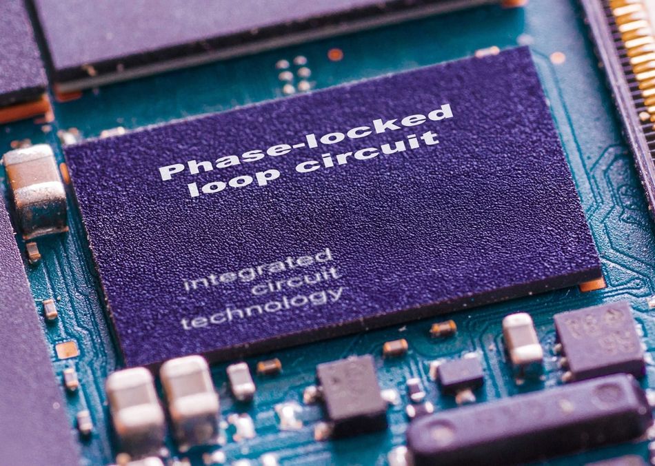
Recommended reading: Phase Locked Loop (PLL): How It Works and How to Design One
Clock and data recovery
Clock and data recovery (CDR) circuits extract timing information from high-speed serial data. The recovered clock must track changes in the incoming data rate while adding as little timing uncertainty as possible.
A VCXO can serve as the controlled oscillator in a CDR loop. The recovered phase information drives the control voltage, which adjusts the VCXO's oscillation frequency until the local clock aligns with the incoming data.
The limited pull range is useful here because the expected data-rate variation is normally small. A wideband VCO could provide more tuning range, but the additional tuning sensitivity and phase noise may be undesirable in a precision clock-recovery system.
The required pull range depends on the interface and timing standard. It should be calculated from the maximum expected transmitter frequency error, reference tolerance, temperature effects, and other system-level errors rather than selected from a generic VCXO specification.
Jitter attenuation and clock cleanup
VCXOs are widely used in jitter attenuators and clock-cleaning circuits. A typical architecture places the VCXO inside a narrowband PLL between a noisy input clock and a clean output clock.
The PLL allows low-frequency frequency variations to pass to the VCXO while attenuating higher-frequency phase variations from the incoming clock. The VCXO therefore acts as the low-noise timing element that determines much of the quality of the cleaned clock.
The loop bandwidth is central to this behavior. A narrower loop can provide stronger attenuation of high-frequency input jitter, but it also responds more slowly to frequency changes. A wider loop tracks frequency variations more quickly but allows more input jitter to reach the output.
The VCXO's own phase noise, Kv, and tuning range must therefore be considered together with the PLL loop bandwidth. A low-noise VCXO cannot compensate for a poorly designed loop or a noisy control-voltage path.
Telecom timing and network synchronization
Network synchronization systems require clocks at different locations to maintain a defined frequency and phase relationship. VCXOs are useful because they can make small frequency corrections while retaining the stability of a quartz reference.
Telecommunications equipment has historically used hierarchical timing architectures in which local oscillators must meet specified frequency accuracy, stability, and holdover requirements. Standards and specifications such as Telcordia GR-1244 define performance requirements for synchronization equipment, although the exact oscillator architecture depends on the equipment class and implementation.
In a synchronization system, the VCXO can be disciplined by an external reference. If the reference is temporarily lost, the oscillator enters holdover, where it continues operating from its local frequency estimate. The oscillator's temperature stability, aging, and short-term noise then become important because they determine how quickly the local clock drifts away from the last valid reference.
This creates a design trade-off between pullability and free-running stability. A VCXO needs enough APR to follow the reference while it is available, but excessive sensitivity can make the oscillator more susceptible to control-node noise. For demanding network synchronization, designers may therefore use a VCXO, VCTCXO, or OCXO depending on the required stability and holdover performance.
Audio and video clocking
Digital audio and video systems are sensitive to clock jitter because timing errors can affect sampling and data conversion. VCXOs can provide low-jitter clock sources for applications such as audio converters, broadcast equipment, video processing, and professional digital interfaces.
In an audio system, for example, the oscillator's phase noise and integrated jitter can contribute directly to the timing uncertainty of the sampling clock. A low-jitter VCXO can therefore be used in a clock-cleaning PLL to isolate the converter from noise on an upstream clock.
Video systems have similar requirements. High-speed pixel and serial-data interfaces often require clocks with controlled phase noise and frequency stability. The required output frequency can range from relatively low reference clocks to hundreds of megahertz, depending on the interface and clock-generation architecture.
The important specification is not simply a low phase-noise number at one offset frequency. Designers should evaluate the complete phase-noise profile and integrated jitter over the bandwidth relevant to the converter or interface.
Instrumentation and precision timing
Test and measurement equipment often requires a stable clock that can be synchronized to an external reference. VCXOs provide a useful combination of frequency stability, electronic tuning, and low phase noise for these applications.
For example, a frequency counter or signal analyzer may use a VCXO inside a PLL so that its local clock can track an external reference. The VCXO provides the fine frequency correction while the PLL determines how quickly and how accurately the local oscillator follows the reference.
Applications that require substantially higher long-term stability may instead use an OCXO (oven-controlled crystal oscillator). An OCXO can provide much lower frequency drift, but at the cost of higher power consumption, warm-up time, and physical size.
Narrowband frequency modulation
A VCXO can also be used as a source of controlled narrowband frequency modulation. An analog modulation signal can be applied to the control input, producing a corresponding change in oscillation frequency.
For small deviations, the instantaneous frequency can be approximated as:
f(t) ≈ f0 + Kv × vC(t)
where:
f(t) = instantaneous output frequency
f0 = nominal output frequency
Kv = tuning sensitivity in Hz/V
vC(t) = time-varying control voltage
This approach is useful when the required frequency deviation is small and the application benefits from the stability of a crystal resonator. However, the VCXO's limited pull range and nonlinear tuning characteristic restrict the amount of modulation that can be applied.
For larger frequency excursions, a VCO is normally more appropriate. A VCO can provide a much wider frequency range, while a VCXO is better suited to applications where frequency stability and low phase noise are more important than wideband tuning.
Clock generators and synchronization systems
VCXOs are also used as the reference element in clock generators and timing ICs. A clock generator can use a VCXO as its low-noise source and then employ frequency dividers, multipliers, or a PLL to produce several synchronized output frequencies.
This architecture allows one stable oscillator to support multiple clock domains. The generated outputs can use interfaces such as LVCMOS (Low-Voltage Complementary Metal-Oxide-Semiconductor), LVDS (Low-Voltage Differential Signaling), LVPECL (Low-Voltage Positive Emitter-Coupled Logic), or HCSL (High-Speed Current-Steering Logic), depending on the system requirements.
In these applications, the VCXO does not necessarily determine the final output frequency directly. Instead, it provides the stable, tunable reference from which the clock generator derives the required frequencies.
The same architecture is common in network synchronization, where a system may need several phase-related clocks with different frequencies and output formats. The VCXO provides the controlled timing reference, while the downstream clock-generation circuitry handles frequency multiplication, division, distribution, and output formatting.
Choosing the right application architecture
The common feature across these applications is the need for controlled frequency correction without sacrificing the stability and low phase noise associated with a quartz resonator. This makes the VCXO particularly effective when the expected frequency correction is small but continuous synchronization is required.
A VCXO is therefore a strong candidate for PLLs, CDR systems, jitter attenuators, clock generators, and network synchronization equipment. A TCXO (temperature-compensated crystal oscillator) may be preferable when temperature stability is the primary requirement and electronic tuning is limited or unnecessary. An OCXO becomes attractive when the system requires substantially higher frequency stability or holdover performance.
The selection should ultimately be based on the complete timing budget. Designers should consider APR, Kv, frequency stability, temperature range, aging, phase noise, integrated jitter, control-voltage noise, PLL bandwidth, and required output frequency together rather than optimizing a single oscillator specification in isolation.
How to Choose or Design with a VCXO
Selecting a VCXO starts with the system's timing requirements. The key is to choose enough tuning capability without adding unnecessary sensitivity to noise.
Set the frequency and output format: Define the required output frequency and select an interface such as LVCMOS (Low-Voltage Complementary Metal-Oxide-Semiconductor), LVDS (Low-Voltage Differential Signaling), or LVPECL (Low-Voltage Positive Emitter-Coupled Logic).
Calculate the required APR: Include reference error, initial tolerance, temperature variation, aging, and other applicable frequency errors. Choose sufficient absolute pull range (APR) with a reasonable margin rather than simply selecting the largest available range.
Select Kv and control voltage: Confirm that the available control voltage matches the PLL, DAC, or loop-filter output. Choose the lowest Kv that provides the required tuning range because higher Kv increases sensitivity to control-voltage noise.
Check stability and jitter: Compare temperature stability, aging, phase noise, and integrated jitter against the system budget. If tighter frequency stability is required, consider a TCXO (temperature-compensated crystal oscillator), VCTCXO, or OCXO (oven-controlled crystal oscillator).
Verify dynamic performance: For PLLs, CDRs, or frequency modulation, check the tuning linearity and modulation bandwidth against the required loop response.
Check package and layout: Confirm the package, supply voltage, control-input characteristics, crystal requirements, and recommended PCB layout. Good decoupling and isolation of the control node are essential for low-jitter operation.
Modern Alternatives and Future Trends
Quartz VCXOs remain important in precision timing, but MEMS resonators, digital frequency control, and integrated PLLs are expanding the available design options. These approaches can provide wider tuning ranges, digital programmability, smaller packages, or improved temperature compensation.
MEMS VCXOs and integrated PLLs
MEMS-based oscillators replace the quartz resonator with a micromachined resonator integrated with silicon circuitry. Some devices combine the resonator with an integrated PLL, allowing the oscillator to provide substantially wider frequency adjustment than a conventional quartz VCXO.
This architecture can also provide programmable frequency, tuning sensitivity, and output formats in a single device. The wider tuning range makes MEMS solutions attractive when a quartz VCXO cannot provide sufficient APR. However, designers should compare phase noise, jitter, temperature stability, aging, and power consumption rather than selecting a MEMS device solely for its wider pull range.
Digitally controlled crystal oscillators
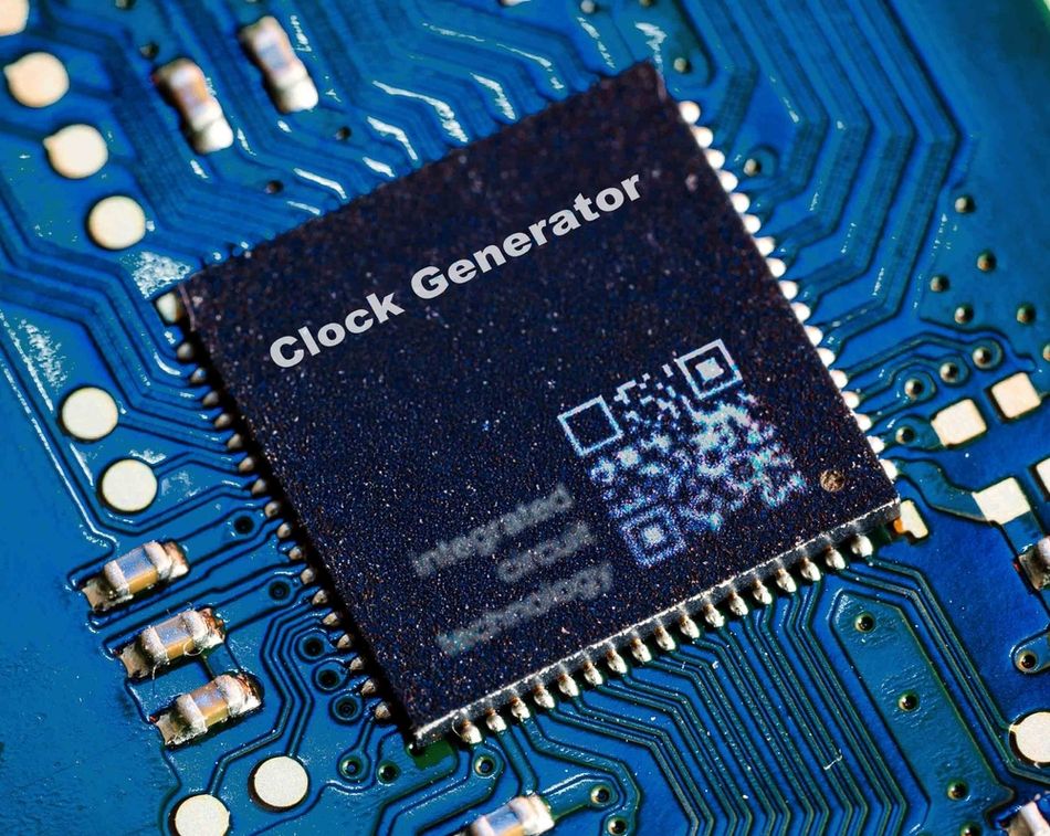
A DCXO (digitally controlled crystal oscillator) replaces the continuous analog tuning input with a digital frequency-control word. Internal switched-capacitor networks or other digital tuning elements adjust the effective capacitance of the crystal circuit.
DCXOs are useful when a microcontroller, FPGA, or digital synchronization algorithm already controls the frequency. Digital control also enables repeatable calibration and avoids some of the noise and drift associated with an external analog control voltage.
The trade-off is resolution and update behavior. The designer must consider tuning step size, frequency quantization, update rate, and the phase noise introduced by the digital control mechanism.
VC-TCXOs and VC-OCXOs
A VCTCXO (voltage-controlled temperature-compensated crystal oscillator) combines the frequency stability of a TCXO with electronic frequency adjustment. This makes it useful when a system needs both temperature compensation and enough tuning capability for synchronization or calibration.
A VC-OCXO (voltage-controlled oven-controlled crystal oscillator) adds electronic tuning to an OCXO. The oven maintains the crystal near a controlled temperature, while the control input provides fine frequency adjustment. This combination can support demanding reference and holdover applications, but the higher power, warm-up time, and larger package can limit its use in compact systems.
Recommended reading: OCXO Design Guide: Oven Controlled Crystal Oscillator
VCSOs and SAW-based oscillators
VCSOs (voltage-controlled surface-acoustic-wave oscillators) use a SAW resonator instead of quartz. SAW technology can support high operating frequencies and can be useful where conventional crystal oscillators become difficult to implement.
Their suitability depends strongly on operating frequency, phase-noise requirements, temperature stability, and tuning range. They should therefore be evaluated against quartz and MEMS alternatives using the complete timing budget rather than frequency range alone.
Programmable and software-defined timing
Modern clock generators increasingly combine resonators, PLLs, fractional frequency synthesis, digital control, and temperature compensation in a single device. This allows one component to generate multiple programmable output frequencies and support different timing standards.
Programmable VCXOs and clock generators can reduce the need for separate oscillator variants and simplify product configuration. Digital control can also support automatic calibration and network synchronization functions.
The long-term trend is toward increasingly integrated timing devices that combine a stable resonator with digital compensation, frequency synthesis, monitoring, and multiple clock outputs. However, conventional quartz VCXOs remain valuable where low phase noise, predictable analog tuning, and simple PLL integration are more important than maximum tuning range or programmability.
Conclusion
A VCXO (voltage-controlled crystal oscillator) provides a practical balance between frequency stability, low phase noise, and fine electronic frequency control. Its quartz resonator limits the tuning range, but this same high-Q resonator provides the stability needed in PLLs, clock recovery, jitter attenuation, and network synchronization systems.
The key design parameters are absolute pull range (APR), Kv, control-voltage range, linearity, frequency stability, phase noise, and jitter. Engineers should select the smallest tuning range and Kv that meet the system's frequency-correction requirements while keeping the control path and power supply sufficiently quiet.
Quartz VCXOs remain a strong choice when predictable analog tuning and low-jitter performance are priorities. MEMS VCXOs, DCXOs, VCTCXOs, and integrated clock generators offer alternatives for wider tuning, digital control, temperature compensation, or higher integration. The right choice ultimately depends on the complete timing budget rather than any single oscillator specification.
FAQ
Q1: Why is the tuning range of a VCXO limited compared with a VCO?
A VCXO uses a high-Q quartz resonator, whose frequency can only be shifted over a relatively small range by changing its effective load capacitance. The crystal's motional parameters and capacitance ratio limit this pulling capability. A VCO (voltage-controlled oscillator) typically uses an LC, ring, or other electronically tunable resonator and can therefore provide a much wider frequency range, but usually with lower frequency stability.
Q2: What is the difference between total pull range and absolute pull range (APR)?
Total pull range describes the frequency excursion obtained as the control voltage moves across its specified range under defined conditions. Absolute pull range (APR) accounts for frequency errors such as initial tolerance, temperature variation, aging, and other specified effects. For PLL design, use the manufacturer's APR definition rather than assuming that total pull range is equivalent to usable correction range.
Q3: How do I select the correct tuning slope (Kv)?
Start by calculating the required frequency correction and available control-voltage range. For an approximately linear tuning curve:
Kv ≈ Required frequency excursion / Usable control-voltage excursion
If frequency is expressed in ppm:
Kv(ppm/V) ≈ Required tuning range(ppm) / ΔVC(V)
Choose the lowest Kv that provides sufficient correction. A higher Kv increases sensitivity to noise on the control-voltage input.
Q4: How does control-voltage noise affect VCXO phase noise and jitter?
Noise on the control voltage produces frequency modulation through the oscillator's tuning characteristic. For small disturbances:
Δf ≈ Kv × vn
where vn is the control-voltage disturbance, and Kv is expressed in Hz/V. Increasing Kv therefore increases the frequency disturbance produced by a given control-node noise level. Low-noise control circuitry, appropriate filtering, careful PCB routing, and a suitable Kv can reduce this contribution to phase noise and jitter.
Q5: Why do datasheets specify best-straight-line (BSL) linearity?
BSL linearity describes how closely the frequency-versus-control-voltage characteristic follows a best-fit straight line across the specified tuning range. It indicates how much the actual tuning response deviates from the idealized relationship.
For PLL applications, the local or incremental tuning sensitivity can also matter, as the effective Kv may change with the control voltage. Designers should therefore review the manufacturer's complete tuning characteristics when accurate loop modeling is required.
Q6: What differentiates VCXOs from VCTCXOs and VC-OCXOs?
A VCXO provides electronic frequency control using a crystal resonator. A VCTCXO (voltage-controlled temperature-compensated crystal oscillator) adds temperature compensation, providing better frequency stability over temperature while retaining electronic tuning. A VC-OCXO (voltage-controlled oven-controlled crystal oscillator) combines an oven-controlled crystal with a tuning input, providing high-frequency stability and fine electronic adjustment for demanding reference and holdover applications.
Q7: Can a VCXO be used for frequency modulation or spread-spectrum clocking?
Yes, provided the required modulation depth and rate remain within the device's specified tuning range and modulation bandwidth. The frequency response can be approximated by:
f(t) ≈ f0 + Kv × vC(t)
However, the tuning characteristic may become nonlinear near the limits of the control-voltage range. For large frequency excursions or highly agile modulation, a VCO or PLL-based synthesizer is generally more appropriate.
Q8: What are the advantages of MEMS-based VCXOs over traditional quartz devices?
MEMS VCXOs use micromachined resonators and can integrate frequency synthesis, digital control, and temperature compensation in a compact package. Some devices provide substantially wider tuning ranges than conventional quartz VCXOs and offer programmable frequency and tuning characteristics.
MEMS technology can also provide strong resistance to mechanical shock and vibration. However, performance varies significantly between devices. Designers should compare phase noise, jitter, frequency stability, aging, power consumption, and temperature performance rather than assuming that MEMS is inherently better than quartz for every timing application.
References
[1] Wenzel Associates, Inc., “Voltage Controlled Crystal Oscillators (VCXOs),” Wenzel Associates, Inc. [Online]. Available:https://wenzel.com/library/crystal-oscillator-tutorials/vcxos-voltage-controlled-crystal-oscillators/ [Accessed: Aug. 26, 2026].
[2] SiTime Corporation, “VCXO parameter trade-offs for PLL design,” Application Note AN10021, SiTime Corporation. [Online]. Available: https://www.sitime.com/support/resource-library/application-notes/an10021-vcxo-parameter-trade-offs-pll-design [Accessed: Aug. 26, 2026].
[3] Renesas Electronics Corporation, “VCXO—Absolute Pull Range,” Application Note 847, Renesas Electronics Corporation. [Online]. Available: https://www.renesas.com/en/document/apn/847-vcxo-absolute-pull-range [Accessed: Aug. 26, 2026].
[4] Texas Instruments, “VCXO application guideline for CDCE(L)9xx family,” Application Report SCAA085A, Texas Instruments. [Online]. Available: TI VCXO Application Guideline. [Accessed: Aug. 26, 2026].
[5] SiTime Corporation, “Designing with the SiT39xx family of DCXOs,” Application Note AN10041, SiTime Corporation. [Online]. Available: https://www.sitime.com/support/resource-library/application-notes/an10041-designing-sit39xx-family-dcxos-digitally [Accessed: Aug. 26, 2026].
in this article
1. Key Takeaways2. Introduction3. Principle of Operation and Circuit Architecture4. Key Specifications and Trade-offs5. Comparison with VCOs, TCXOs, OCXOs and Related Devices6. Circuit Design Considerations7. Applications8. How to Choose or Design with a VCXO9. Modern Alternatives and Future Trends10. Conclusion11. FAQ12. References