STM32 Selection Guide: Choosing the Right Part for Your Design
An STM32 microcontroller selection guide built as a working method: narrowing 1,644 parts down to one order code, organized by the constraint that actually drives your design rather than by part number.

03 Sep, 2026. 27 minutes read
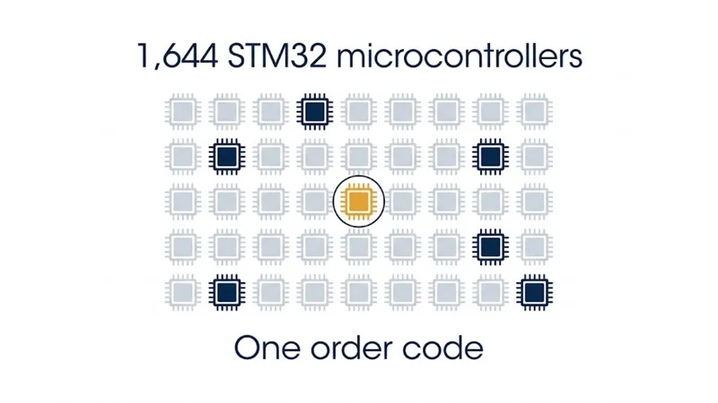
Narrowing 1,644 STM32 microcontrollers to one order code, filtered by design intent.
Key Takeaways
Selection is a filtering problem. ST's portfolio spans more than twenty series and well over a thousand order codes. Name the one constraint that dominates your design: power, cost, throughput, radio, security, AI, or certification, and most of the catalogue disappears before you open a single datasheet. [1]
Series choice is mostly core choice. Cortex-M0+ gives you the lowest power floor. [1] Cortex-M4 adds DSP instructions and a floating-point unit. [7] Cortex-M7 adds caches and throughput. [3] Cortex-M33 adds TrustZone hardware isolation. [8] Cortex-M55 adds Helium vector processing, and on the STM32N6 it sits alongside ST's Neural-ART NPU. [1]
Not every STM32 has a usable internal flash. The STM32H7R/H7S carry 64 KB of user flash and boot from external memory; the STM32N6 is flash-less by design. Choose one of these without planning for it, and you discover a second memory chip, an external loader, and a new boot chain during board layout.
RAM is the binding constraint. Ceilings run from 20 KB on an STM32L0 and up to 40 KB on an STM32U0 to 3 MB on an STM32U5. [1] A single 320×240 display buffer at 16 bits per pixel needs about 150 KB, which eliminates most of the mainstream portfolio in one line.
Package is an early filter. Board area, pitch, and whether your assembler can place and rework a BGA will cut candidates faster than clock speed ever does.
The order code is what you actually buy. In STM32F407VGT6, the suffix encodes pin count, flash size, package, and temperature range. VGT6 and VET6 differ only in flash. ZGT6 is the 144-pin version of the same die, and that one changes your PCB design. [11]
Introduction
Choosing an STM32 microcontroller for modern embedded systems is not hard because the parts are complicated. It is hard because there are so many of them, and because neighboring options often differ by one peripheral or 64 KB of RAM. The datasheets are excellent. The problem is knowing which forty of them to ignore. [1]
This guide is a selection method, not a family introduction. If you need background on what the STM32 family is and how the series relate to each other, start with the STM32 microcontroller pillar guide and come back here when you are ready to pick a part.
Most selection guides answer that by walking the portfolio series by series, which reproduces the problem rather than solving it. This guide does the opposite. It assumes you are designing a real product, that something about that product is non-negotiable, and that naming the non-negotiable thing first is what makes everything after it fast.
That is the method in one line: filter by design intent, in a fixed order, until one order code is left.
How this Guide Works
Selection goes wrong when you start at the end, with a part number you used last time, and reason backwards until it fits. So this guide runs the other way, in three stages.
Narrow. Name the one thing your design can't compromise on: battery life, cost, speed, a radio. A chip built for speed is bad at power, and the reverse, so naming it clears most of the catalogue.
Verify. Check that family actually works for you. Enough working memory, the right connections, a package your assembler can solder. It's easy to pick the right family and still pick a part you can't build with.
Commit. Get to something you can order. Every letter in an STM32 part number means something, and that's where mistakes happen. Decode it, check it's in stock, check it'll still be made in three years.
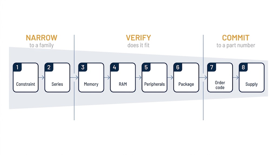
Work through them in that order. Each stage narrows the list, so the further you get, the less there is to compare.
Step 1: Name the Constraint That Dominates
Every design has one thing it can't compromise on. A wearable that has to run a year on a coin cell is a power problem before it's anything else. A motor controller is a timing problem. A camera node running vision models is a compute problem. Name that thing first, and most of the portfolio disappears. Naming it first eliminates roughly 80% of the portfolio immediately.
That trade is real, not marketing. A chip that hits 600 MHz needs a bigger process node, more power, more pins, and a bigger package. A chip that idles at a few microamps clocks slowly, because clocking fast is what costs the power. You cannot have both. So the first decision isn't which chip, it's which compromise you're willing to make.
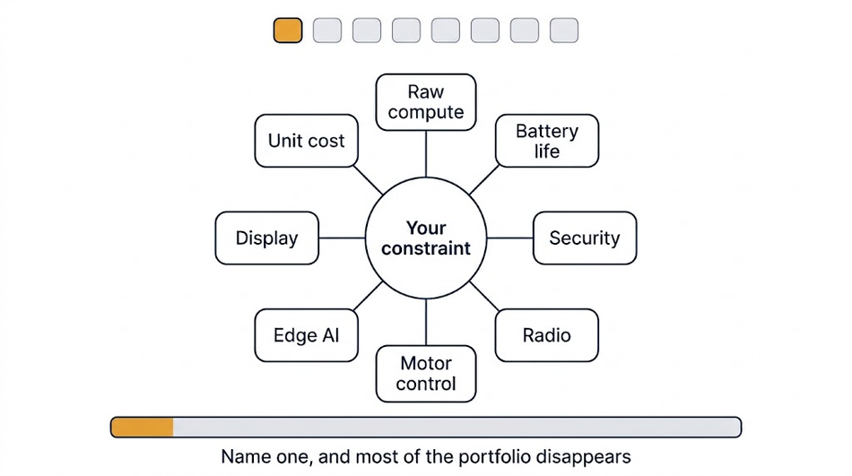
Eight design constraints radiating from a central choice: raw compute, battery life, security, radio, motor control, edge AI, display, unit cost.
Here's where each constraint takes you. [1]
Dominant constraint | Where to look | What you are trading away |
Raw compute | STM32V8, STM32H7, STM32H5, STM32F7, STM32N6 | Power consumption, unit cost, package size |
Battery life | STM32U5, STM32U3, STM32U0, STM32L4, STM32L0 | Clock speed and peak throughput |
Hardware security | Any Cortex-M33 series: STM32H5, STM32L5, STM32U5, STM32U3, STM32C5, STM32WBA [8] | Cost and development time for the secure boot chain |
Integrated radio | STM32WB, STM32WB0, STM32WBA, STM32WL, STM32WL3 | Peripheral breadth and maximum clock speed |
Analog and real-time control | STM32G4, STM32F3 | Memory ceiling and top-end compute |
Edge AI and vision | STM32N6, STM32V8 | Cost, board complexity, external memory |
Large display or graphics | STM32V8, STM32H7, STM32H7R/S, STM32H5, STM32L4+ | Board complexity and often external memory |
Unit cost | STM32C0, STM32G0, STM32C5 | Almost everything else |
When Two Constraints Tie
They often do, and the answer is usually that you've named the constraint too vaguely.
Power and security. The most common tie, and ST built parts for it. The STM32U5 and STM32U3 exist because low-power connected products now have to meet security rules. [4] If you're stuck here, you probably want one of those rather than a low-power part plus an external security chip.
Speed and memory. Anything with a screen ties these. The framebuffer is the memory problem, and the refresh rate is the speed problem, and they're the same problem. Treat it as one constraint: how much data do I have to move, how often.
Cost and certification. This tie usually means the budget is wrong, not the part. Certified silicon costs more, and the cheapest certified option is still more expensive than the uncertified part you were comparing it to.
When a tie is genuine, pick the family that solves the harder constraint and check the other one in Step 4. Memory is easier to verify late than power is.
Tip: If you can't name a dominant constraint, the requirements aren't finished. "Fast, cheap and low power" isn't a specification; it's a wish list, and it will send you round the portfolio twice.
Recommended Reading: Motor Speed Control: Methods Across Motor Types
Step 2: Choose the Series
STMicroelectronics groups the portfolio into mainstream (553 devices), high-performance (515), ultra-low-power (480), and wireless (96).[1] The table below is the whole MCU portfolio in one place.
Series | Core | Max clock | Flash | Best for |
STM32C0 | Cortex-M0+ | 48 MHz | 16 to 256 KB | Replacing an 8-bit part on cost |
STM32C5 | Cortex-M33 | 144 MHz | 128 KB to 1 MB | Entry-level designs that still need TrustZone |
STM32G0 | Cortex-M0+ | 64 MHz | 16 to 512 KB | The modern default for cost-sensitive designs |
STM32F0 | Cortex-M0 | 48 MHz | 16 to 256 KB | Legacy only, use STM32G0 instead |
STM32F1 | Cortex-M3 | 72 MHz | 16 KB to 1 MB | Legacy only, huge community base |
STM32F3 | Cortex-M4 | 72 MHz | 32 to 512 KB | Analog-rich real-time control |
STM32G4 | Cortex-M4 | 170 MHz | 32 to 512 KB | Motor control and digital power |
STM32F2 | Cortex-M3 | 120 MHz | 128 KB to 1 MB | Legacy performance designs |
STM32F4 | Cortex-M4 | 180 MHz | 64 KB to 2 MB | The general-purpose workhorse |
STM32F7 | Cortex-M7 | 216 MHz | 64 KB to 2 MB | Throughput with cache, pre-H7 designs |
STM32H5 | Cortex-M33 | 250 MHz | 128 KB to 4 MB | Performance plus certified security |
STM32H7 | Cortex-M7 (+ Cortex-M4) | 600 MHz (M4 at 240 MHz) | 64 KB to 2 MB | Maximum Cortex-M7 throughput, dual-core split |
STM32H7R/H7S | Cortex-M7 | 600 MHz | 64 KB user flash, boots from external memory | Large displays and external-memory designs |
STM32N6 | Cortex-M55 | 800 MHz | None, boots from external memory | Edge AI and computer vision, with Neural-ART NPU |
STM32V8 | Cortex-M85 | 800 MHz |
| Highest performance, industrial and edge AI. New in 2026 |
STM32L0 | Cortex-M0+ | 32 MHz | 8 to 192 KB | Entry battery designs, packages from 14 pins |
STM32L4 | Cortex-M4 | 80 MHz | 64 KB to 1 MB | Battery designs needing DSP and FPU |
STM32L4+ | Cortex-M4 | 120 MHz | 512 KB to 2 MB | Low-power designs with graphics |
STM32L5 | Cortex-M33 | 110 MHz | 32 to 512 KB | Low power with TrustZone |
STM32U0 | Cortex-M0+ | 56 MHz | 16 to 256 KB | Modern entry-level battery designs |
STM32U3 | Cortex-M33 | 96 MHz | 512 KB to 2 MB | Best-in-class efficiency, DSP and AI tasks |
STM32U5 | Cortex-M33 | 160 MHz | 128 KB to 4 MB | Demanding battery designs with security |
STM32WBA | Cortex-M33 | 100 MHz | 512 KB to 2 MB | Current-generation short-range wireless |
STM32WB | Cortex-M4 + Cortex-M0+ | 64 MHz (M0+ at 32 MHz) | 256 KB to 1 MB | Bluetooth LE, Zigbee, Thread, Matter |
STM32WB0 | Cortex-M0+ | 64 MHz | 192 to 512 KB | Simple Bluetooth LE on a tight battery budget |
STM32WL | Cortex-M4 + Cortex-M0+ | 48 MHz | 64 to 256 KB | LoRaWAN and sub-GHz long range |
STM32WL3 | Cortex-M0+ | 64 MHz | 64 to 256 KB | Sub-GHz metering, asset tracking, remote control |
Cost-driven Designs
The STM32C0 is ST's most cost-effective series: a 48 MHz Cortex-M0+ with 16 to 256 KB of flash and up to 36 KB of RAM, from around $0.21 [2]. It exists to replace 8-bit parts, so if you are moving off a PIC or an AVR, this is the landing spot.
The STM32C5 pushes the entry point up to a 144 MHz Cortex-M33 with up to 1 MB of flash and 256 KB of SRAM, from $0.64 [1]. That is TrustZone at close to entry-level pricing, so reach for it when cost is the constraint but security is also in scope.
Treat the STM32G0 as the default for new cost-sensitive work: a 64 MHz Cortex-M0+ with up to 512 KB of flash and 144 KB of RAM. ST groups the C0, F0, G0 and F1 as highly compatible, so moving between them later costs little [2].
Pick: STM32G0. Fallback: STM32C0 if you are squeezing, STM32C5 if security creeps into scope.
Tip: Design for the G0 footprint even if you fit a C0, and you have a free upgrade path for nothing.
High-performance Designs
The STM32V8 is ST's new performance flagship: an 800 MHz Cortex-M85 with up to 4 MB of embedded phase-change memory, and the first STM32 to pass 5,000 CoreMark at 5,072, roughly 60% ahead of the STM32H7R/S [15]. The M85 brings Helium vector processing, so it handles signal processing and machine learning workloads that would previously have pushed you to an application processor. It also tolerates 140°C junction temperature, which matters in industrial work.
The catch is maturity. It launched in late 2025 with documentation and boards arriving in Q3 2026, so community material and third-party framework support will be thin for a while. Confirm stock and lead time before you design it in.
Performance scales cleanly across the rest of the series, and ST publishes comparable figures [3]:
Series | Benchmark | Notes |
STM32F2 | 150 DMIPS / 398 CoreMark at 120 MHz | 90 nm process, 175 µA/MHz dynamic current |
STM32F4 | 225 DMIPS / 608 CoreMark at 180 MHz | ART Accelerator, eight product lines |
STM32F7 | 462 DMIPS / 1082 CoreMark at 216 MHz | ART Accelerator plus L1 cache |
STM32H7 | 1327 DMIPS / 3347 CoreMark | 600 MHz Cortex-M7, some parts with a second Cortex-M4 at 240 MHz |
STM32V8 | 5,072 CoreMark | 800 MHz Cortex-M85 with Helium, up to 4 MB embedded PCM |
The STM32H7 remains the volume choice: cache, a dual-core split on some lines, and an ecosystem where your RTOS and middleware already work.
The STM32F7 is the previous generation, same architecture at a third the throughput. If your bottleneck is a control loop rather than data processing, it costs less and does the job.
The STM32H5 is the one people miss. Slower on paper, but it carries cryptographic accelerators and certified security services ST maintains over the product's life [3]. If you need fast and certified, it often beats an H7 with a separate security chip bolted on.
Pick: STM32H7 for anything shipping soon. Fallback: STM32V8 if you need the ceiling and can absorb a new part, STM32H5 if certification is in scope, STM32F7 if the H7 is overkill.
Battery-powered Designs
The STM32U3 is the current efficiency leader, and not marginally. ST quotes 117 CoreMark/mW against 53.9 for the STM32U5, roughly double the previous generation, with static consumption around 1 to 2 µA [4]. It is the first STM32 built on near-threshold design, which is where that jump comes from.
It runs a 96 MHz Cortex-M33 with up to 2 MB of flash and 640 KB of RAM on the newer U3B5 and U3C5 parts. It also carries a hardware signal processor, ST's HSP, which ST claims runs ML workloads up to nine times more power-efficiently than a U5 [4]. That is what makes running a model on harvested energy realistic rather than aspirational. For anything on a coin cell, start there.
The STM32U0 is the cheaper entry point at 56 MHz, with up to 256 KB of flash and 40 KB of RAM. That RAM ceiling is the thing to check early.
The STM32U5 is for battery designs that also need real capability: up to 4 MB of flash, up to 3 MB of RAM, a 160 MHz Cortex-M33, and the STM32U585 holds PSA Certified Level 3 and SESIP 3 [4].
The STM32L4 remains relevant at 100 DMIPS with DSP instructions and an FPU, and the L4+ extends that to 120 MHz and 409 CoreMark with up to 2 MB of flash and 640 KB of SRAM [4].
Pick: STM32U3. Fallback: STM32U0 if cost matters more than efficiency, STM32U5 if you need headroom.
Tip: ST keeps the U3 and U5 pin-to-pin compatible within the same package, and the U0 is pin-to-pin with many L0, L1, and L4 packages. Moving within either group is cheap, but the U0 and the U3/U5 are not compatible with each other.
Motor Control and Analog Designs
The STM32G4 is the one to know. A 170 MHz Cortex-M4 with CORDIC and FMAC hardware accelerators for trigonometric and filtering math, which is why it dominates field-oriented motor control [2]. Doing that maths in software costs cycles you do not have inside a control loop, so the accelerators buy you either a faster loop or a better model of the motor.
Memory is the ceiling here, not compute. The G4 gives you up to 512 KB of flash and 128 KB of RAM [2], enough for a control loop and not much else. If your design also needs a display or a network stack, check that before you commit.
The STM32F3 covers the same intent at lower cost and clock speed, with integrated op-amps and fast ADCs, at up to 512 KB of flash and 80 KB of RAM [2].
Pick: STM32G4. Fallback: STM32F3 if the loop is slow enough and cost is tight.
Tip: Count advanced-control timer channels, not total timers. Three-phase control needs complementary outputs with dead-time insertion, and a general-purpose timer will not do it.
Wireless Designs
STM32Wx parts are a radio transceiver and an MCU in one system-on-chip, covering sub-GHz and 2.4 GHz [5]. Pick the protocol first. The protocol decides the silicon, not the other way round.
Protocol | Series | Core | Notes |
Bluetooth LE, Zigbee, Thread, Matter | STM32WBA | 100 MHz Cortex-M33 | Current generation, 40 nm |
Bluetooth LE, Zigbee, Thread, Matter | STM32WB | 64 MHz Cortex-M4 + 32 MHz Cortex-M0+ | Dedicated radio core |
Bluetooth LE only | STM32WB0 | 64 MHz Cortex-M0+ | Cheapest BLE route |
LoRaWAN, Sigfox, sub-GHz | STM32WL | 48 MHz Cortex-M4, dual-core lines add a Cortex-M0+ | Long range |
Sub-GHz metering, remote control | STM32WL3 | 64 MHz Cortex-M0+ | Newer sub-GHz line |
Prefer the STM32WBA over the STM32WB for new designs unless you need a specific WB feature. The 40 nm process is why its power figures are better [5].
The dual-core split matters more than it first appears. On the STM32WB, the radio stack runs on a dedicated Cortex-M0+ while your application owns the Cortex-M4, so application code cannot break protocol timing [5]. On single-core parts, you take on that scheduling risk yourself.
For sub-GHz, the STM32WL and STM32WL3 are different series, not variants of each other. The WL is the LoRaWAN part, with longer range and more memory. The WL3 is a newer Cortex-M0+ line for metering, asset tracking, and remote control, with less memory at lower cost.
Pick: STM32WBA for short range, STM32WL for LoRaWAN. Fallback: STM32WB0 if it is Bluetooth LE only and cost is tight, STM32WL3 for simpler sub-GHz work.
Tip: Budget design time for the radio section of the board as well as the firmware. Antenna matching and RF layout are where integrated-radio designs go wrong, and no amount of code fixes a badly matched antenna.
Recommended Reading: RF PCB: Materials, Impedance Control, Manufacturing, and 5G mmWave Design Guide
Edge AI and Vision Designs
Two answers, and they solve the problem differently.
The STM32N6 puts a dedicated neural processing unit on the die: an 800 MHz Cortex-M55 with ST's Neural-ART accelerator, 4.2 MB of RAM and an image signal processor [1]. If your workload is vision, this is purpose-built for it.
The STM32V8 runs AI on the core instead, using the Cortex-M85's Helium vector instructions. ST claims up to six times the DSP and ML throughput of an H7 [15]. No dedicated NPU, but 4 MB of embedded memory and general-purpose performance the N6 does not have.
The practical split: dedicated vision workloads point at the N6, mixed workloads where AI is one job among several point at the V8.
A third route, if the model is small and power matters more than throughput: the STM32U3's hardware signal processor runs machine learning on an ultra-low-power part [4]. Keyword spotting and simple classification fit there. Vision does not.
One thing to plan for on the N6: it has no internal flash, so your program lives on a separate memory chip. Step 3 covers what that costs you. Not a reason to avoid the part, but a reason not to discover it at layout.
Pick: STM32N6 for vision. Fallback: STM32V8 if AI is one workload among several, STM32U5 if the workload turns out lighter than expected.
Designs with a Display
Displays tie two problems together. The framebuffer eats memory and the refresh rate eats throughput, and you cannot solve one without the other.
Start with the arithmetic. A 320x240 screen at 16 bits per pixel needs about 150 KB for a single buffer, 300 KB double-buffered, before your application exists. That number alone eliminates most of the mainstream portfolio.
The STM32H7 handles most screens with 1.4 MB of RAM on board [1]. The STM32H5 gives you up to 4 MB of flash for assets, which matters when your images and fonts are bigger than your code [3].
For larger or higher-resolution screens, the STM32H7R/H7S exists specifically for this: a 600 MHz Cortex-M7 with 64 KB of user flash and 620 KB of SRAM, built to run from external memory, with a graphics line (H7R7/H7S7) carrying ST's NeoChrom GPU. Same caveat as the N6: external memory is part of the design, not an option.
The STM32V8 also carries graphics hardware: Chrom-ART, a JPEG codec and an LCD controller alongside 4 MB of embedded memory [15]. Worth considering at the top end if you are already looking at it for compute.
At the low end, the STM32L4+ runs small displays on a battery at 120 MHz with up to 640 KB of RAM [4].
Pick: STM32H7 for most screens. Fallback: STM32H7R/S when the framebuffer will not fit internally, STM32L4+ if it is a small display on a battery.
Security-critical Designs
Security here means TrustZone, Arm's hardware isolation between trusted and untrusted code [8]. It is a property of the Cortex-M33, so the requirement narrows you to the M33 series immediately: STM32H5, STM32L5, STM32U5, STM32U3, STM32C5 and STM32WBA.
Which one depends on your other constraints, because they span the portfolio. Cheap and secure is the C5. Battery and secure is the U3 or U5. Fast and secure is the H5. Wireless and secure is the WBA.
If you need a certificate rather than just the hardware, check parts rather than series. The STM32U585 holds PSA Certified Level 3 and SESIP 3 [4]. Certification is granted per part, so never assume it carries across a series.
Functional safety is separate. If you are building to IEC 60730 or IEC 61508, ST publishes safety packages with self-test libraries and certification artefacts. These are series- and part-specific, so check your candidate has one before you commit.
Pick: depends on your second constraint. Use the four pairings above.
Step 3: Check the Memory Architecture
You have a family. Before you size anything, check what kind of memory the chip actually has, because on a few STM32s the answer is "not much, and not where you expect."
There are three arrangements.
Embedded flash. The normal one. Program lives in internal flash and runs from there. This covers almost the whole portfolio, from the C0 to the U5.
Bootflash. A small internal flash holds a bootloader, and your application lives on an external memory chip. The STM32H7R and H7S work this way, with 64 KB of user flash and 620 KB of internal SRAM [13].
Flashless. No flash at all. ST defines these as products with contiguous embedded RAM and a fast serial interface out to external memory [13]. The STM32N6 is one.
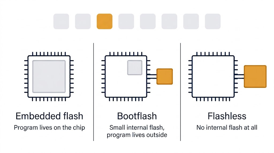
What the last two cost you
- Your BOM grows.
- Your board gets harder.
- Your project structure changes. ST splits a bootflash application into three parts: boot code in internal flash, application code in external flash, and a separate external memory loader. That last one is a project in its own right, generated in STM32CubeMX [14].
- Your performance ceiling moves. External memory typically runs at half or a third of the core clock, so on graphics work the memory bus becomes the bottleneck before the CPU does. An 800 MHz core does not help if the pixels arrive at 200 MHz.
The Tooling Exists
ST ships two pieces of middleware, the External Memory Manager and the External Memory Loader, both in STM32CubeMX under Middleware and Software Packs [13]. The manager gives you one API across memory types and a boot system that launches your application from external memory. Application note AN6101 covers the flow [14].
Tip: If you are considering an H7R/S or an N6, build the STM32CubeMX bootflash project before you commit. It takes an afternoon and tells you what you are signing up for while changing your mind is still free.
Step 4: Size Flash Memory and RAM
Flash sizes are advertised, RAM is where designs actually fail. Check RAM against your real requirement before you commit to a series.
What Each Series Gives You
Sorted by ceiling, so you can find your number and read across.
RAM ceiling | Series |
4.2 MB | STM32N6 |
3 MB | STM32U5 |
1536 KB | STM32H5 |
1.4 MB | STM32H7 |
640 KB | STM32L4+, STM32U3 |
620 KB | STM32H7R/H7S |
512 KB | STM32F7, STM32WBA |
384 KB | STM32F4 |
320 KB | STM32L4 |
256 KB | STM32C5, STM32L5, STM32WB |
144 KB | STM32G0 |
128 KB | STM32F2, STM32G4 |
96 KB | STM32F1 |
80 KB | STM32F3 |
64 KB | STM32WB0, STM32WL |
40 KB | STM32U0 |
36 KB | STM32C0 |
32 KB | STM32F0, STM32WL3 |
20 KB | STM32L0 |
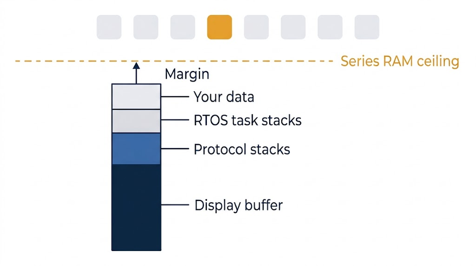
These are ceilings, not typical values [1]. RAM also does not track flash within a series, so once you have a candidate part number, take the figure from that part's datasheet and nothing else.
Working Out Your Number
Four things dominate, and most people account for the first and forget the rest.
Your own data. Buffers, lookup tables, application state.
Display buffers. This dwarfs everything. A 320x240 screen at 16 bits per pixel is about 150 KB for one buffer, 300 KB double-buffered, before a line of your code exists.
Protocol stacks. TCP/IP, Bluetooth, USB. Each wants tens of kilobytes, and none of it tunes away later.
RTOS task stacks. Every task gets its own, so RAM scales with task count, not code size. Ten tasks at 2 KB each is 20 KB that appears nowhere in your source.
Add those up, then add a twenty to thirty percent margin. The feature that arrives in month six always needs memory.
Tip: Size for the product you will ship, not the prototype. The prototype has no logging, no OTA buffer, and no error handling, and all three cost RAM.
If you are within ten percent of the ceiling, move up within the series first. Usually the same footprint, a different order code.
Step 5: Verify the Peripheral Set
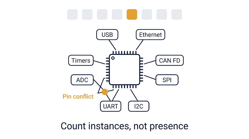
By this point you have a series. Now confirm the specific device carries the peripherals you need, in the quantity you need. This is where a candidate usually dies quietly. Not because the peripheral is missing from the series, but because it is missing from the part you picked, or because two peripherals you need share the same pins.
Serial Interfaces
Nearly every STM32 offers SPI, I2C, and UART [1]. What varies is how many instances, and whether they support the speeds you need. Count instances, not presence.
Recommended Reading: I2C vs SPI vs UART: A Comprehensive Comparison
USB
Full-speed and high-speed are different peripherals, and high-speed often needs an external PHY. Some STM32C0 parts run USB without an external crystal, saving a component on cost-driven designs [2].
Ethernet
The fastest filter here. Most STM32s have no Ethernet MAC, so this requirement collapses the portfolio to a handful of series. Check it first if it applies.
CAN and CAN FD
Classic CAN caps payloads at 8 bytes; FD carries 64 and runs faster in the data phase, so if you are moving firmware updates over the bus, FD is what you want. FD support is narrower than CAN support, with the STM32G4 the obvious example [2]. Every interface also needs an external transceiver on the board.
Timers
Advanced-control timers with complementary outputs and dead-time insertion are what make three-phase motor control practical. Count advanced-control channels, not total timers. Background on PWM signals is worth reading before you compare timer blocks.
ADC and Analog
Resolution, sampling rate, and channel count vary widely. The STM32F3 and STM32G4 add integrated op-amps and comparators, which can remove components from your BOM [2].
External Memory Interfaces
If you landed on a bootflash or flashless part in Step 3, confirm the interface here. XSPI, FMC, and SDMMC differ in width and speed, and on graphics work, the interface sets your ceiling, not the core clock.
DMA
Easy to overlook, hard to add later. Running out of channels forces interrupt-driven workarounds that cost you the performance you bought the part for.
GPIO
Count usable pins, not total pins. A 64-pin part does not give you 64 free I/O once your SPI, UART, and timer outputs are placed.
Clocking
Decide early between an external crystal and the internal oscillator. USB, CAN and radio protocols usually force a crystal, which is a component and a footprint to plan for [2].
Debug
SWD is universal. Trace output is not, and losing it on timing-sensitive work is painful to discover late.
Do this in STM32CubeMX, not on paper
Configure your pinout in STM32CubeMX before committing to a package. It knows which alternate functions collide, so it shows conflicts a datasheet table hides. It also includes a power consumption calculator, useful on a battery design before hardware exists [6].
Tip: Build the pinout for the part you think you want, then add the two peripherals you might need later. If it still routes, you have headroom.
One thing you do not need to factor in: the toolchain. STM32CubeIDE supports every STM32 MCU and MPU [6].
Recommended Reading: Crystal Oscillator: Fundamentals, Models, and Design Guidelines
Step 6: Confirm the Package Fits
You have a part that does everything you need. Now check you can physically build with it.
Package gets treated as a detail at the end, encoded in a letter of the order code. In practice, it eliminates candidates as hard as memory does, for reasons that have nothing to do with the silicon.
Four Questions
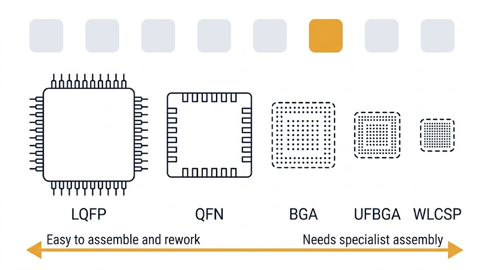
Does it fit the board? An LQFP144 occupies roughly four times the area of an LQFP48 once you account for the lead span. Package area decides pin count, and pin count decides which peripherals you can route out.
Can your assembler place it? BGA and WLCSP have contacts underneath the body. Not every assembly house handles them, and the ones that do charge more.
Can it be reworked? If a board fails test, someone has to lift the chip. On an LQFP that is routine. On a BGA it needs specialist equipment, with a good chance the board is scrapped instead.
Can your fab do the pitch? Fine-pitch packages need tighter track and gap tolerances, and often more layers to escape the pins. A 0.4 mm pitch BGA can push a two-layer design to four.
What the Packages Mean
Code | Package | Notes |
T | LQFP | Leads around the edge, easy to assemble and rework. The default |
U | UFQFPN or VFQFPN | Smaller, no leads, pads underneath the edge. Reworkable with care |
H | BGA | Contacts under the body. Smallest area for the pin count, hardest to assemble |
I | UFBGA | Ultra-fine-pitch BGA |
Y | WLCSP | Chip-scale. Smallest option, and the most demanding on assembly and PCB |
P | TSSOP | Through the low pin-count range only |
Codes are defined per datasheet, so confirm against the one for your part [11]. Step 7 explains why.
Pin count is not usable I/O
A 100-pin part is not 100 free pins. Power, ground, crystal, debug and every peripheral you enabled take physical pins first. Build the pinout in STM32CubeMX and count what is left.
Voltage and Temperature
Both eliminate parts as fast as the package does.
Supply voltage. Most STM32s run from around 1.7 V to 3.6 V. If your system is 5 V, you need level shifting or a regulator, and you need to know whether the specific pins you are using are 5 V tolerant. Tolerance is per pin, not per chip.
Temperature grade. The order code carries it: 6 is industrial up to 85 °C, 7 extends to 105 °C [11]. Pick the grade your enclosure needs, then check Step 8, because higher grades stock more thinly.
Tip: Ask your assembly house what they can place before you finalize the package. A five-minute email occasionally saves a re-spin.
When Package Wins
Sometimes the package decides the part. A wearable with 15 mm of board space is a WLCSP problem first and a microcontroller problem second, so find the smallest package that carries your peripherals and work backwards.
If that happens, go back to Step 2 with package as your dominant constraint.
If nothing in the portfolio fits, that is a signal worth taking seriously. Programmable logic may be the better answer.
Recommended Reading: FPGA vs Microcontroller: Understanding the Key Differences and Use Cases
Step 7: Decode the Order Code
A series gets you to a family. The order code gets you to a purchasable part. The suffix encodes pin count, flash size, package, and temperature range [11].
Take STM32F407VGT6. The front half, STM32F407, is what people say out loud. You cannot order it, because dozens of parts share that name. The suffix is what makes it specific:
V — 100 pins
G — 1024 KB of flash
T — LQFP package
6 — industrial temperature, −40 to 85 °C
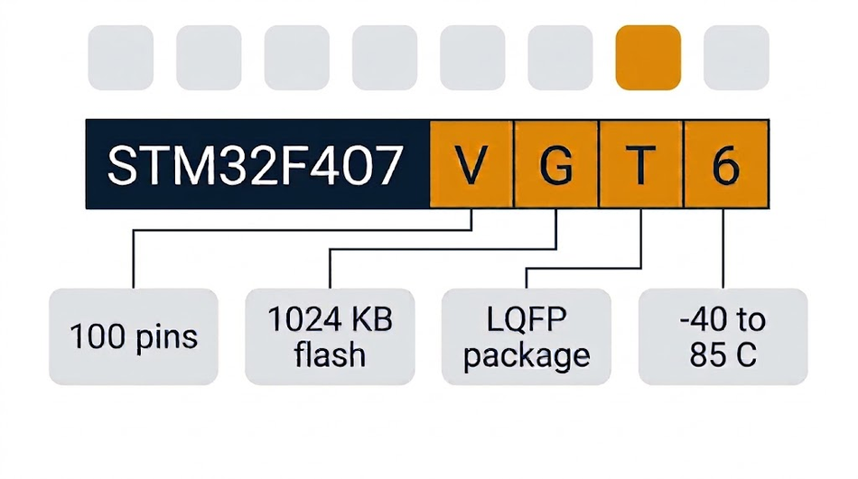
Change one character and you get a physically different chip.
Read the codification from the datasheet, not a universal key
ST publishes an ordering information scheme in each datasheet, and the letters are defined per document rather than across the portfolio. In the STM32F103 medium-density datasheet, ST defines only four pin-count letters (T = 36, C = 48, R = 64, V = 100) and two flash codes (8 = 64 KB, B = 128 KB), because those are the only variants at that density [11].
The table below is a cross-family guide. The datasheet governs a purchase order.
Field | Codes |
Pin count | F = 20, G = 28, K = 32, T = 36, S = 44, C = 48, R = 64, V = 100, Z = 144, I = 176 |
Flash size | 4 = 16 KB, 6 = 32 KB, 8 = 64 KB, B = 128 KB, C = 256 KB, D = 384 KB, E = 512 KB, F = 768 KB, G = 1024 KB, H = 1536 KB, I = 2048 KB |
Package | T = LQFP, H = BGA, U = VFQFPN, P = TSSOP, Y = WLCSP. ST's F103 datasheet also defines I = UFBGA, and gives U as VFQFPN or UFQFPN[11] |
Temperature | 6 = industrial, -40 to 85 °C; 7 = industrial, -40 to 105 °C[11] |
Options (trailing) | Blank for standard product, additional letters (e.g., R, TR, T) often indicate packing (reel, tape & reel) or qualified/customer variants; check the datasheet for your family. |
The same letter can mean different things in different families or positions, so always confirm against the ordering information table for your part [11].
Worked Example: the STM32F407 Variants
This is the comparison engineers most often get wrong, because the codes look similar:
Order code | Pin count | Flash memory | Package | Temperature |
STM32F407VGT6 | 100 | 1024 KB | LQFP | -40 to 85 °C |
STM32F407VET6 | 100 | 512 KB | LQFP | -40 to 85 °C |
STM32F407ZGT6 | 144 | 1024 KB | LQFP | -40 to 85 °C |
Read that as two independent decisions.
VGT6 against VET6 is purely a flash decision on the same 100-pin footprint. If 512 KB is enough, drop to the VET6 and save the cost.
VGT6 against ZGT6 is purely a pin-count decision, and it changes your PCB: 144 pins need more escape routing and often another layer.
Tip: Paste the full order code into your schematic symbol and your BOM, not the short name. "STM32F407" in a BOM is an invitation to order the wrong one.
Recommended Reading: What is a Multilayer PCB?
Step 8: Confirm Availability and Long-Term Supply
A part that is perfect and unobtainable is not a selection. Five checks before committing.
Stock and lead time for the exact order code, not the base part.
Temperature grade. The 105 °C variants are consistently thinner on stock than the 85 °C ones.
Lifecycle status. ST classifies parts as active, NRND or obsolete, and the middle one is the one people miss. NRND means not recommended for new designs: the part still ships and ST still honors its longevity commitment, so an existing product is fine, but do not start there. The STM32L1 is the current example.
Longevity. ST runs a 10-year longevity program and publishes the list of parts it covers [12]. Check it if your product has a long life.
A pin-compatible fallback within the same series. This is the practical benefit of ST's compatible-series design [2]. For alternatives outside the STM32 family, Findchips has a guide to STM32 second sourcing.
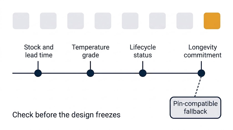
Capture that fallback in your schematics as a documented alternate, not in someone's head. When a line goes on allocation, the teams that recover fastest are the ones whose schematics already name a second source and whose firmware compiles for it.
Legacy is not the same as unavailable
ST lists the STM32F0 and STM32F1 as legacy [2]. They are excellent for learning, widely documented and still stocked everywhere. That is a learning argument, not a design-in argument. Starting a new product on a legacy part forgoes better performance per unit cost and shortens your runway before the next migration.
New parts have the opposite problem
The STM32V8 launched in late 2025, with documentation and boards through Q3 2026 [15]. It is real and fast, but community examples, third-party support and reference designs take time to appear. The same applies to the U3, C5, WB0 and WL3.
RTOS support is part- and board-specific and can lag first silicon, so check the board support list for Zephyr or FreeRTOS before you commit.
Tip: Before the design freezes, run a two-minute check: exact order code in stock at two distributors, lifecycle status active, on the longevity list if you need it, and a named fallback in the schematic.
From requirement to order code: a full walkthrough
The examples above stop at a series. This one runs all the way to a purchase order.
The design. A connected industrial gateway in a cabinet. Sensor data over CAN, a local web interface over Ethernet, a small status display over SPI. Mains powered, ten-year product life, volumes in the low thousands.
Step 1: the constraint. Power is irrelevant, and cost will not decide it. What decides it is whether the thing serves a network stack and handles CAN traffic without dropping frames. Throughput, with memory close behind.
Step 2: the series. Throughput routes to high-performance, and the STM32H7 is the pick. The H5 is worth a look because ten-year industrial life often brings security requirements, but no certification is in scope here.
Step 3: memory architecture. The H7 has embedded flash, so nothing changes on the BOM. Worth confirming, because the neighboring H7R/S does not.
Step 4: RAM. TCP/IP wants roughly 50 KB. A dozen RTOS task stacks add a few tens more. Application buffers for CAN and logging, call it 200 KB. Around 350 KB, plus margin, so 450 KB. That rules out everything below the H7 except the F7, and the F7 at 512 KB leaves no room to grow over ten years. The H743 specifically gives you 1 MB, comfortably clear
Step 5: Peripherals. Ethernet MAC, which eliminates most of the portfolio in one filter. Two CAN FD, two SPI, one I2C, two UARTs. The pinout routes in STM32CubeMX, but not on a 100-pin part once Ethernet's RMII pins are placed.
Step 6: Package. The pin count rules out the 100-pin variants. LQFP144 fits, and the assembly house handles it without special tooling. Temperature grade 6 is enough for a cabinet.
Step 7: the order code. H743 line, 144 pins, 2 MB flash, LQFP, industrial. Z for 144 pins, I for 2048 KB, T for LQFP, 6 for −40 to 85 °C, giving STM32H743ZIT6. Confirm every letter against that part's datasheet before releasing the order. Worth noting the H743 runs at 480 MHz, not the 600 MHz the series table gives: series pages carry ranges, datasheets carry the part.
Step 8: Supply. The exact code is stocked at multiple distributors, around £13 for a single unit and closer to £10 at 250 up. Check the grade you need is the one stocked, lifecycle status is active, and the part is on ST's longevity list. Then name a fallback with the same footprint in the schematic.
What the method did. Step 1 removed the low-power and cost families. Step 2 narrowed to one series. Step 4 removed everything below the H7. Step 5 removed the parts without Ethernet. Step 6 removed the 100-pin variants. By Step 7, a handful remained, and the order code chose between them.
One thing that would have changed the answer. If that display were a 480x272 color touchscreen, the framebuffer alone would need about 261 KB per buffer, and you would want an LTDC controller rather than bit-banging over SPI. The H743 has no LTDC. The H7A3 and H7B3 lines do, with 1.4 MB of RAM, Chrom-ART and a JPEG codec, in the same LQFP144 package. That makes STM32H7A3ZIT6 the answer instead, or the H7B3 if you also need crypto and Secure Firmware Install. "The H7 series does displays" is true of the series and false of some parts in it.
Common Selection Mistakes
Starting from a part number you have used before. Familiarity is a real benefit, but a five-year-old choice usually has a cheaper, faster, current-generation equivalent.
Sizing flash and forgetting RAM. Still the most common error. Flash is advertised, RAM is what runs out, and it runs out late.
Assuming every STM32 has usable internal flash. The STM32H7R/S has 64 KB and boots from external memory. The N6 has none. Choosing one without planning for it means discovering a second memory chip during layout.
Treating package as a late decision. Whether your assembler can place a BGA, and whether a failed board can be reworked, eliminates candidates as hard as memory does.
Ignoring the legacy label. The STM32F0 and F1 are excellent for learning and widely documented, but ST classifies both as legacy [2]. Designing a new product around them forgoes better performance per unit cost.
Assuming a new series has mature support. The STM32V8, U3 and C5 are very recent, and the WB0 and WL3 still have thinner ecosystems than the core F, H and U lines. Check your stack supports the part first.
Choosing a wireless part before the protocol. Bluetooth LE, Zigbee, Thread and LoRaWAN map to different series [5]. The protocol constrains the silicon, not the other way round.
Assuming pin count equals usable I/O. Alternate function conflicts routinely cost you pins you assumed you had. Check in STM32CubeMX.
Reading only the series page. Series pages give ranges. Datasheets give the actual figures for the actual part, and within a series the variation is large.
Conclusion
STM32 selection is a filtering process, and the order of the filters is what makes it fast. Name the dominant constraint, route it to a series, check the memory architecture, size RAM honestly, verify peripherals in STM32CubeMX, confirm the package fits, decode the order code, then check supply.
Most of these decisions are reversible. ST keeps peripherals, drivers, and tooling consistent across series and several series pin-compatible, so a requirements change late in development usually means a different part rather than a different vendor.
Frequently Asked Questions
How do I choose between STM32F4 and STM32H7?
Choose the F4 if your bottleneck is a control loop, the H7 if it is data processing. The F4 delivers 608 CoreMark at 180 MHz with up to 384 KB of RAM; the H7 reaches 3347 CoreMark at 600 MHz with up to 1.4 MB [3]. The F4 costs less. If you need certification alongside performance, check the H5.
What is the difference between the STM32 F series and G series?
The G series is the modern replacement. The G0 supersedes the F0 at 64 MHz with up to 144 KB of RAM; the G4 supersedes the F3 at 170 MHz, adding CORDIC and FMAC accelerators. ST lists the F0 and F1 as legacy [2].
Which STM32 has the lowest power consumption?
The STM32U3, built on near-threshold design and quoted at 117 CoreMark/mW [4]. For entry-level battery designs where cost matters more, start at the U0.
Which STM32 is the fastest?
The STM32V8, at 5,072 CoreMark on an 800 MHz Cortex-M85 [15]. The N6 follows at 3,360 and the H7 at 3,347. It launched in late 2025 with boards in Q3 2026, so confirm stock before designing it in.
Which STM32s need external flash?
The H7R, H7S and N6. The H7R and H7S carry 64 KB for a bootloader and run the application from external memory; the N6 has none at all [13]. All three need an external memory chip, a boot chain and a memory loader, which ST supports in STM32CubeMX.
Which STM32 has an NPU?
The STM32N6, using ST's Neural-ART accelerator alongside an 800 MHz Cortex-M55 [1]. It is the only STM32 with a dedicated NPU. The V8 runs AI on the core using Helium instead.
What is the difference between the STM32WL and STM32WL3?
Separate series, not variants. The WL is the LoRaWAN part, a 48 MHz Cortex-M4 with up to 256 KB of flash. The WL3 is a newer 64 MHz Cortex-M0+ line for sub-GHz metering and asset tracking, with 16 to 32 KB of RAM at lower cost [5].
What do the letters at the end of an STM32 part number mean?
Pin count, flash size, package and temperature. In STM32F407VGT6: V is 100 pins, G is 1024 KB, T is LQFP, 6 is −40 to 85 °C. ST defines these per datasheet, so confirm against your part's ordering table before ordering [11].
Do I need a Cortex-M33 part?
Only if you need TrustZone, Arm's hardware isolation between trusted and untrusted software [8]. That narrows you to the H5, L5, U5, U3, C5 or WBA. Certification is per part, not per series: the STM32U585 holds PSA Certified Level 3 and SESIP 3 [4].
Can I migrate between STM32 series later?
Usually yes. ST treats the C0 and G0 as pin-to-pin compatible, and the F0 and F1 as another pair, though the two pairs are not compatible with each other. Peripherals and HAL drivers stay consistent, so migration costs far less than changing vendor [2].
How many STM32 microcontrollers are there?
ST lists 1,644 as of August 2026: 553 mainstream, 515 high-performance, 480 ultra-low-power and 96 wireless [9].
References
[1] STMicroelectronics, "STM32 32-bit Arm Cortex MCUs." [Online]. Available: https://www.st.com/en/microcontrollers-microprocessors/stm32-32-bit-arm-cortex-mcus.html. [Accessed: Aug. 31, 2026].
[2] STMicroelectronics, "STM32 mainstream MCUs." [Online]. Available: https://www.st.com/en/microcontrollers-microprocessors/stm32-mainstream-mcus.html. [Accessed: Aug. 31, 2026].
[3] STMicroelectronics, "STM32 high performance MCUs." [Online]. Available: https://www.st.com/en/microcontrollers-microprocessors/stm32-high-performance-mcus.html. [Accessed: Aug. 31, 2026].
[4] STMicroelectronics, "STM32 ultra low power MCUs." [Online]. Available: https://www.st.com/en/microcontrollers-microprocessors/stm32-ultra-low-power-mcus.html. [Accessed: Aug. 31, 2026].
[5] STMicroelectronics, "STM32 wireless MCUs." [Online]. Available: https://www.st.com/en/microcontrollers-microprocessors/stm32-wireless-mcus.html. [Accessed: Aug. 31, 2026].
[6] STMicroelectronics, "STM32U0 series." [Online]. Available: https://www.st.com/en/microcontrollers-microprocessors/stm32u0-series.html. [Accessed: Aug. 31, 2026].
[7] STMicroelectronics, "STM32H7R/H7S series." [Online]. Available: https://www.st.com/en/microcontrollers-microprocessors/stm32h7-series.html. [Accessed: Aug. 31, 2026].
[8] Arm Ltd., "Cortex-M33." [Online]. Available: https://www.arm.com/products/silicon-ip-cpu/cortex-m/cortex-m33. [Accessed: Aug. 31, 2026].
[9] STMicroelectronics, "STM32 MCU product selector." [Online]. Available: https://www.st.com/en/microcontrollers-microprocessors/stm32-32-bit-arm-cortex-mcus/products.html. [Accessed: Aug. 31, 2026].
[10] STMicroelectronics, "STM32CubeIDE." [Online]. Available: https://www.st.com/en/development-tools/stm32cubeide.html. [Accessed: Aug. 31, 2026].
[11] STMicroelectronics, "STM32F103x8, STM32F103xB medium-density performance line datasheet," DS5319 Rev. 20, Sec. 7, "Ordering information scheme."
[12] STMicroelectronics, "Product longevity commitment." [Online]. Available: https://www.st.com/content/st_com/en/about/quality-and-reliability/product-longevity.html. [Accessed: Aug. 31, 2026].
[13] STMicroelectronics, "Getting started with External Memory Manager and External Memory Loader," STM32 MCU wiki. [Online]. Available: https://wiki.st.com/stm32mcu/wiki/Getting_started_with_External_memory_Manager_and_External_memory_loader. [Accessed: Aug. 31, 2026].
[14] STMicroelectronics, "Introduction to external memory manager and external memory loader middleware for boot flash MCU," Application Note AN6101, Rev. 1, 2024.
[15] STMicroelectronics, "STM32V8 series: new generation of high-performance MCUs," product presentation. [Online]. Available: https://www.st.com/resource/en/product_presentation/stm32v8-presentation.pdf. [Accessed: Aug. 31, 2026].
in this article
1. Key Takeaways2. Introduction3. Step 1: Name the Constraint That Dominates4. Step 2: Choose the Series5. Step 3: Check the Memory Architecture6. Step 4: Size Flash Memory and RAM7. Step 5: Verify the Peripheral Set8. Step 6: Confirm the Package Fits9. Step 7: Decode the Order Code10. Step 8: Confirm Availability and Long-Term Supply11. From requirement to order code: a full walkthrough12. Common Selection Mistakes13. Frequently Asked Questions14. References