Understanding PCB Thickness: A Comprehensive Guide
PCBs are extensively used across industries, powering devices from simple gadgets to complex systems. In this article, we’ll understand the importance of PCB thickness, the various factors affecting it, and its impact on design and other factors.

Last updated on 21 Feb, 2024. 16 minutes read
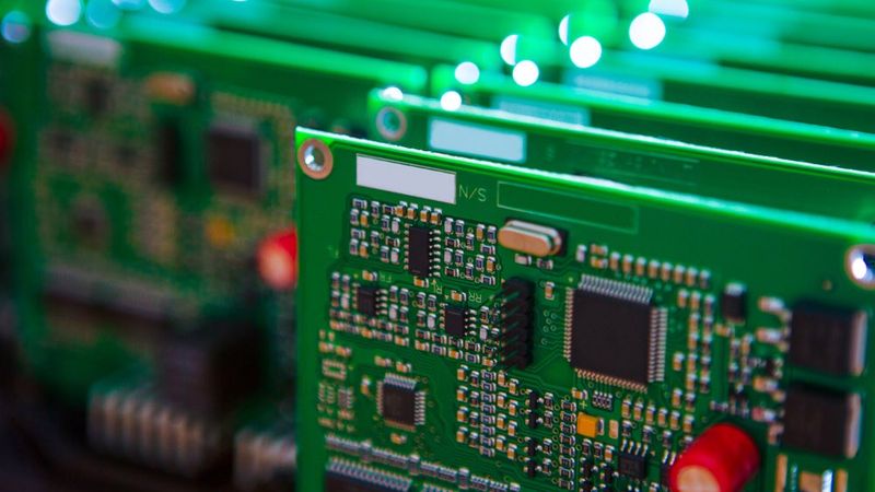
Multiple PCBs
Introduction
Printed Circuit Boards (PCBs) are the backbone of electronic devices, providing a platform for various components and facilitating interconnections between them. One critical aspect of PCB design is the board thickness. PCB thickness plays a pivotal role in the overall performance and reliability of the electronic device it supports. It influences several factors, including the board's mechanical strength, thermal management capabilities, and the manufacturing process. Therefore, understanding PCB thickness is crucial for anyone involved in designing or manufacturing electronic devices. This article aims to provide a comprehensive understanding of PCB thickness, factors affecting PCB thickness, its impact on manufacture and performance, and its role in hear dissipation.
Basics of PCB
A Printed Circuit Board (PCB) is a thin board made of composite material, such as fiberglass or composite epoxy. The primary function of a PCB is to provide a physical base upon which to mount the electronic components of a system. It also provides the necessary conductive pathways for electrical signals to travel between these components. These pathways, known as traces, are typically made of copper and are embedded in the surface of the PCB.
The design of a PCB involves several critical parameters, including the number and arrangement of layers, the layout of components, and the routing of traces. However, one often overlooked yet important parameter is the PCB thickness.
Importance of PCB in Electronics
PCBs are integral to modern electronic devices. They provide the necessary infrastructure for mounting and interconnecting various electronic components, such as resistors, capacitors, and integrated circuits. Without PCBs, these components would need to be connected manually, leading to complex and unreliable wiring arrangements. The use of PCBs in electronics manufacturing has several advantages:
- They allow for a high degree of miniaturization, enabling the creation of compact and lightweight electronic devices.
- They ensure repeatability and consistency in manufacturing, leading to high-quality and reliable products.
- They allow for easy troubleshooting and repair, as the layout of components and connections is clearly defined and standardized.
PCB thickness plays a crucial role in these advantages. It directly impacts the mechanical strength of the board, its thermal performance, and manufacturability. Therefore, understanding and correctly specifying PCB thickness is critical to PCB design and manufacturing.
What is Standard PCB Thickness?
PCB thickness refers to the overall thickness of the PCB board, including the base material and all the layers of copper, solder mask, and silkscreen. It is typically measured in millimeters (mm) or inches. The PCB thickness can vary depending on the application, but most standard PCBs used in consumer electronics have a thickness of 1.6mm, approximately 0.063 inches.
The industry has adopted it for several reasons:
A thickness of 1.6mm provides a good balance between mechanical strength and weight. A thicker PCB board would be stronger and heavier, which could disadvantage portable devices.
A thickness of 1.6mm is compatible with most through-hole components, which have leads designed to fit through holes in the board. If the board were thicker, the leads might not be long enough to go through the board and be soldered on the other side.
A thickness of 1.6mm is relatively easy to manufacture. It is thick enough to be handled without too much risk of breaking but not so thick that it causes problems in the manufacturing process. For example, when drilling holes in the board, a thicker board would require longer drill bits and more time to drill each hole.
However, it's important to note that though 1.6mm is the standard thickness for many PCBs, it is not the only option. A few more common PCB thickness selections emerged, including 2.36mm (93 mils) and 3.17mm (125 mils). These values, among others, constitute the range of standardized PCB thickness.
PCBs can be made thinner or thicker depending on the application's specific requirements. For example, PCBs used in high-power applications may be thicker to improve their thermal performance, while PCBs used in ultra-compact devices may be thinner to save space.
Factors Influencing PCB Thickness
In the intricate world of Printed Circuit Board (PCB) design and manufacturing, the thickness of the PCB plays a pivotal role in determining its performance, durability, and suitability for specific applications. Various factors, as discussed below, intricately influence this crucial aspect, each contributing to the final characteristics and capabilities of the board.
Substrate Thickness
The substrate (or base material), often made from materials like FR4 (a composite of woven fiberglass and epoxy resin), polyimide, or CEM, acts as the foundational layer of the PCB. Its primary role is to provide mechanical support and rigidity to the board, ensuring durability and resistance against physical stresses.
The choice of substrate material and its thickness are critical decisions impacting the PCB's ability to withstand thermal stress, mechanical impact, and environmental conditions. In general, substrate thickness can vary widely depending on the application.
For instance, a thicker substrate (closer to 0.125 inches (3.2 mm)) may be preferred for enhanced structural robustness, which is ideal for heavy-duty or automotive applications where the PCB may be subjected to significant mechanical stress. Conversely, in applications where space is a premium – such as in smartphones or wearable technology – a thinner substrate (around 0.031 inches (0.8 mm) to 0.04 inches (1.0 mm)) is desirable to reduce the overall size and weight of the device.
Prepreg Thickness
Prepreg is a dielectric material that provides insulation between two cores or between a core and a copper foil in a PCB. It is also called a binding material, an insulation layer that binds two cores or a core and a copper foil. Prepreg is a major element of multilayer PCBs. The basic functions of prepregs include binding a core to another core, binding a core to a layer, providing insulation, and protecting a multilayer board from short-circuiting.
Prepreg is made with a combination of fiberglass and a resin bonding agent. The fiberglass is pre-impregnated with the resin bonding agent, which is how the name 'prepreg' came about. This impregnation is usually done with epoxy-based materials or partially cured polyimides to create prepreg materials.
There are three main types of prepreg based on the amount of resin present: high resin (HR), medium resin (MR), and standard resin (SR). The thickness of a Prepreg material depends on the amount of resin content bound with the glass fiber. Therefore, high resin makes for thicker and more expensive prepreg materials.
Moreover, prepreg thickness and resin content regulate the impedance, drilling, etching quality, dielectric constant, and Coefficient of Thermal Expansion (CTE).
In PCB fabrication, the prepreg is sandwiched between two copper layers and then stacked, heated, and pressed to create a laminate. Laminates are regarded as the core of a PCB, which serves to bind, strengthen, and protect the layers of a PCB. The prepreg thickness used in a multilayer board varies according to the overall thickness of the PCB board. They can be pp-106 (0.002 inches or 0.0508 mm), pp-1080 (0.003 inches or 0.0762 mm), pp-2113(0.004 inches or 0.1016 mm), and pp-2116 (0.0047 inches or 0.1194 mm).
PCB Copper Thickness
The copper thickness used in PCB production is generally measured in ounces. The standard copper thickness is 1 oz. A specific copper weight is evenly spread on a board to cover 1 square foot to determine the thickness. Therefore, the resulting foil thickness of 1 oz of copper rolled out over 1 square foot will be 0.0348 mm or 1.37 mils.
Copper thickness plays an essential role in the overall thickness of the PCB [1]. The current carrying capacity of a PCB is determined by the thickness of its copper traces and, therefore, of the copper layer. For boards with impedance control, the required trace width is a significant determinant of how thick the copper should be. Other important factors include the PCB weight, component compatibility requirements, and the type of connectors that will be assembled onto the board.
In relation to this, the internal layer (or inner layers of a multilayer PCB) indicates the vertical distance between the copper-tracked layers of a PCB. The circuit board's specific construction sequences determine the internal layers' thickness. The copper weight and thickness are customizable according to the application requirements. The copper weight in the layer determines the minimum trace width and spacing that can be produced.
In circuits where the current requires more thickness, copper would be added as required. It is worth noting, however, that this process is quite complex and time-consuming.
Multi-Layer PCB Thickness
A multilayer PCB has more than two layers in its stack-up configuration [2][3]. Each PCB layer is essentially a level of conductive material, such as copper, for signal routing, separated by insulating material or dielectric, which prevents electrical shorts between the conductive layers. As the number of layers increases to accommodate more complex circuit designs, additional signal routing, or specific power and ground planes, the overall thickness of the PCB also increases.
This increase in thickness is attributed to the added conductive and insulating layers and the need for prepreg layers, which act as adhesive and insulation between the copper layers. These multilayer designs are essential for advanced electronic applications that require high-density interconnections, improved signal integrity, and reduced electromagnetic interference.
However, with each additional layer, the manufacturing process becomes more complex and costly, and the board becomes physically thicker, which may not be desirable in all applications. Designers must carefully consider the trade-offs between the complexity of the circuit, the physical space available, and the impact on the PCB's thickness and cost.
Solder Mask Thickness
The solder mask is a critical layer applied to the surface of a Printed Circuit Board (PCB) to protect the copper traces from oxidation and prevent solder bridging during component soldering. While its thickness is relatively minor compared to the overall PCB thickness, it still contributes to the total thickness of the board. A thicker solder mask can offer better protection against environmental factors and mechanical wear but may affect the precision of soldering small components due to reduced pad clearance. Balancing solder mask thickness is essential for ensuring the PCB's durability and the accuracy of component placement and soldering processes.
In conclusion, the thickness of a PCB is determined by a combination of factors, including the substrate thickness, prepreg thickness, PCB copper thickness, number of layers, and the thickness of the solder mask and silkscreen layers. By understanding these factors, PCB designers can make informed decisions about the thickness of their boards to meet the requirements of their specific applications.
Suggested Reading: PCB Layers: Everything You Need to Know
Suggested Reading: PCB Soldermask: Everything You Need to Know
Importance of PCB Thickness
The thickness of a PCB is a critical parameter that affects various aspects of the board's performance and reliability. It influences the mechanical strength of the board, its thermal performance, and manufacturability. A well-designed PCB with the appropriate thickness can ensure optimal performance and longevity of the electronic device it supports.
PCB Thickness and Device Performance
- Thermal Management: PCB thickness directly correlates with its ability to manage heat. Thicker PCBs have a larger thermal mass, allowing them to dissipate heat more effectively than thinner boards. This is particularly important in high-power applications or in compact devices where heat accumulation can affect performance and longevity. Designers must consider the balance between thickness and thermal requirements to prevent overheating and ensure stable operation.
- Signal Integrity: In high-speed digital circuits, the PCB's thickness can influence the transmission lines' impedance, which further affects signal quality. A thicker PCB can provide better impedance control, reducing signal reflections and crosstalk and accurately transmitting high-speed signals.
- Mechanical Strength: PCB thickness can also impact the mechanical strength of the board, which is particularly important in devices subject to physical stress or vibration. Thicker PCBs are generally more robust and resistant to bending or warping, which is crucial for applications subjected to mechanical stress or harsh environmental conditions. However, increased thickness can also make the board heavier and less flexible, considerations that must be balanced based on the application's specific mechanical requirements.
- Electrical Conductivity: While the thickness of the conductive copper layer is a more direct measure of electrical conductivity, the overall PCB thickness can also play a role. In multilayer PCBs, the thickness and arrangement of layers can affect the distribution of power and ground planes, impacting the board's electrical performance. Optimizing PCB thickness can help in achieving the desired electrical characteristics and performance.
In summary, the thickness of a PCB plays a crucial role in the performance and reliability of electronic devices. By understanding the impact of PCB thickness on thermal management, signal integrity, and mechanical strength, designers can make informed decisions about the appropriate thickness for their specific applications.
PCB Thickness and Manufacturing Process
The thickness of a PCB not only affects the electronic device's performance and significantly impacts the manufacturing process. Manufacturing PCBs with non-standard thicknesses can introduce challenges and complexities that must be addressed to ensure a high-quality and reliable end product.
- Drill Holes: One of the primary challenges in manufacturing PCBs with non-standard thicknesses is drilling holes for through-hole components and vias. Thicker PCBs require longer drill bits and increased drilling time, leading to higher manufacturing costs and longer production times. Additionally, drilling holes in thicker PCBs can increase the risk of drill bit breakage and reduce the accuracy of the hole placement.
- Lamination Complexity: Another challenge in manufacturing PCBs with non-standard thicknesses is the increased complexity of the lamination process. To form a cohesive board, the lamination process involves pressing multiple copper and insulating material layers under high temperatures and pressure. Thicker PCBs may require additional pressure and longer lamination times to ensure proper bonding between the layers. This can also increase the risk of defects, such as delamination or warping, compromising the board's integrity.
- Etching: The etching process used to create the conductive paths on the PCB can be affected by the board's thickness. Thicker PCBs, especially those with thicker copper layers, may require longer etching times and more aggressive chemicals to remove unwanted copper. This can increase the risk of under-etching or over-etching, potentially compromising the precision of the circuit patterns and impacting the board's overall quality.
- Assembly: Thicker boards require increased heat application and prolonged soldering durations to form solder joints properly. This intensified heat exposure raises the risk of thermal damage, potentially affecting the delicate components mounted on the board and the structural integrity of the PCB itself. In PCB Assembly, ensuring the balance between adequate heat for soldering and preventing thermal damage is paramount.
- Depanelization Method: PCB thickness also influences the choice of the depanelization method, which separates individual boards from a larger panel after manufacturing. Thicker PCBs may require more robust depanelization methods, such as routing or sawing, compared to thinner boards that can be separated using scoring or laser cutting. The selected depanelization method must be compatible with the PCB's thickness to minimize stress on the boards and prevent damage during separation.
In conclusion, the thickness of a PCB plays a crucial role in the manufacturing process, and designers must carefully consider the implications of their chosen thickness on the manufacturability of the board. By understanding the challenges associated with non-standard PCB thicknesses, designers can make informed decisions that balance performance requirements with manufacturing constraints.
Suggested Reading: PCB Manufacture Process: A Comprehensive Guide to Understanding and Mastering the Techniques
Suggested Reading: PCBA vs PCB: The foundation of modern-day electronics
Choosing the Right PCB Thickness
Selecting the appropriate PCB thickness is a critical aspect of the design process, as it can significantly impact the electronic device's performance, reliability, and manufacturability. Designers must carefully consider various factors, such as the application requirements, manufacturing constraints, and cost considerations, to determine the optimal thickness for their specific project.
Considerations for High-Frequency Applications
In high-frequency applications, the choice of PCB thickness becomes even more critical, directly affecting signal integrity and overall device performance. Several factors must be taken into account when selecting the appropriate thickness for high-frequency PCBs:
- Impedance: The PCB's thickness, the dielectric constant of the substrate material, and the copper traces' width determine the transmission lines' characteristic impedance. Maintaining a consistent impedance across the entire length of the transmission line is crucial for minimizing signal reflections and ensuring accurate signal transmission. Designers must carefully choose the PCB thickness to achieve the desired impedance while considering other factors, such as mechanical strength and thermal performance.
- Signal Attenuation: Thicker PCBs can increase dielectric losses, leading to signal attenuation and reduced signal quality. Designers must balance the need for a thicker PCB to achieve better mechanical strength and thermal performance with the potential for increased signal attenuation.
- Electromagnetic Shielding: Thicker PCBs can provide better shielding against electromagnetic interference (EMI), which can be particularly important in applications with sensitive components or circuits. Designers must weigh the benefits of improved EMI shielding against the potential drawbacks, such as increased weight and manufacturing complexity.
In conclusion, choosing the right PCB thickness for high-frequency applications requires a careful evaluation of various factors, including impedance control, signal attenuation, electromagnetic shielding, mechanical strength, and thermal performance. By considering these factors, designers can make informed decisions resulting in high-performance, reliable, cost-effective electronic devices.
Considerations for High-Power Applications
When designing PCBs for high-power applications, the thickness of the board becomes a critical factor to consider. High-power circuits generate significant amounts of heat, and the PCB must be capable of dissipating this heat effectively to prevent overheating and potential damage to the components. A thicker PCB can provide better heat dissipation, as it has a larger surface area for heat to spread and dissipate.
- Thermal Resistance: However, a thicker PCB also has a higher thermal resistance, making it less efficient at transferring heat from the components to the surrounding environment. This can lead to higher operating temperatures for the components, reducing their lifespan and reliability. Therefore, designers must carefully balance the need for effective heat dissipation with the potential drawbacks of increased thermal resistance.
- Copper Layer Thickness: The thickness of the copper layers on the PCB determines how much current the board can safely carry. A thicker PCB can accommodate thicker copper layers, carrying more current without overheating. However, thicker copper layers also increase the weight and cost of the PCB, so designers must consider these factors when choosing the appropriate PCB thickness.
- Higher Voltages: High-power applications often involve higher voltages, increasing the risk of arcing and electrical breakdown. A thicker PCB can provide better insulation between the layers and reduce the risk of electrical breakdown. However, it can also increase the size and weight of the device, which may not be desirable in certain applications.
In conclusion, choosing the right PCB thickness for high-power applications involves carefully evaluating various factors, including heat dissipation, current carrying capacity, electrical insulation, and the size and weight of the device. By considering these factors, designers can make informed decisions resulting in high-performance, reliable, cost-effective electronic devices.
The Importance of PCB Thickness in Heat Dissipation
As electronic devices become increasingly compact and powerful, generating heat becomes a significant challenge, necessitating innovative solutions to prevent overheating and ensure reliability and longevity. The thickness of a Printed Circuit Board (PCB) plays a pivotal role in addressing these thermal management challenges.
Impact of PCB Thickness on Heat Dissipation
- Thermal Conductivity: One of the primary advantages of a thicker PCB is its enhanced thermal conductivity. A thicker board facilitates a more even distribution of heat across its surface, aiding in the reduction of hotspots and improving the overall thermal management of the device. This characteristic is crucial for maintaining the temperature of heat-generating components within safe operational limits, thus preventing damage and potential failure.
- Mechanical Support for Heat Sinks: A thicker PCB provides superior mechanical support for components and heat sinks, which is vital for devices generating substantial heat. The robust structure ensures that heat sinks and other thermal management solutions remain securely attached, optimizing their effectiveness in heat removal and contributing to the stability and durability of the device.
- Increased Surface Area: The potential for a greater surface area with a thicker PCB also contributes to improved heat dissipation. In situations where design constraints limit the size of heat sinks or rely on natural convection for cooling, the increased surface area of a thicker PCB can offer significant benefits, enhancing the device's ability to shed heat effectively.
Factors Influencing Optimal Thickness for Heat Dissipation
The determination of optimal thickness for effective heat dissipation in PCBs is influenced by many factors. This subsection delves into how these variables interact to shape the design considerations for maximizing thermal efficiency and device longevity.
- Material Composition: The choice of materials in PCB construction plays a significant role in thermal management. For its high thermal conductivity, materials such as copper are essential for traces and vias, facilitating efficient heat dissipation. Selecting materials with superior thermal properties can improve the PCB's ability to manage heat.
- Layer Count: The thickness of a PCB, influenced by its layer count, affects thermal pathways within the board. Incorporating more layers allows for the addition of dedicated thermal planes, which can significantly enhance heat distribution and dissipation, making the layer count a critical consideration in thermal management strategies.
- PCB Layout and Design: Effective thermal management is also a function of the PCB's design and layout. Strategic placement of components, traces, and vias can optimize thermal paths, improving the board's heat dissipation capabilities. A well-considered design ensures that heat is efficiently transferred away from critical components, maintaining operational stability.
Suggested Reading: How to Design a PCB Layout: A Comprehensive Guide
Solutions for Optimizing PCB Thickness for Heat Dissipation
Optimizing the thickness of Printed Circuit Boards (PCB) for heat dissipation is crucial in enhancing the reliability and performance of electronic devices. This subsection explores various strategies and materials that can be employed to improve thermal management through careful PCB design and thickness optimization.
- Material Selection: Opting for PCB materials with high thermal conductivity is a straightforward approach to enhance heat dissipation. Incorporating materials like Aluminum and Copper as heat spreader layers can significantly improve thermal performance, addressing the heat management needs of high-power devices.
- Thermal Vias: Thermal vias are crucial in transferring heat from hot components to a heat dissipation layer or across the PCB. They are especially beneficial in multilayer PCBs, where thermal pathways must traverse several layers, facilitating effective heat management.
- Heat Sinks and Cooling Solutions: Beyond optimizing PCB thickness, integrating external cooling solutions such as heat sinks, fans, or even liquid cooling systems can provide additional avenues for heat management, further enhancing the device's ability to maintain optimal temperatures.
- Simulation and Testing: Employing thermal simulation software in the design phase allows for predicting heat flow and identifying potential hotspots. This enables design adjustments, including modifications to PCB thickness, to ensure efficient heat dissipation is achieved in the final product.
- Collaboration with Manufacturers: Engaging with PCB manufacturers early in the design process can offer insights into the capabilities and limitations of various materials and thickness options. This collaboration is invaluable in identifying the most effective thermal management solutions, ensuring that the chosen PCB thickness contributes positively to the device's thermal performance.
By carefully considering the impact of thickness on thermal conductivity [4], mechanical support for thermal management components, and the overall surface area available for heat dissipation, designers can significantly improve the thermal management of electronic devices[5]. Coupled with strategic material selection, design, and the incorporation of external cooling solutions, optimizing PCB thickness becomes a cornerstone of effective thermal management strategies in electronics design.
Conclusion
Understanding PCB thickness is essential for designing and manufacturing high-quality, reliable electronic devices. The thickness of a PCB affects various aspects of its performance, including thermal management, signal integrity, and mechanical strength. Designers must carefully consider the application requirements, manufacturing constraints, and cost considerations when selecting the appropriate PCB thickness. By employing accurate measurement techniques and tools, designers and manufacturers can ensure their PCBs meet the required specifications and perform as intended.
FAQs
Q: What is the standard thickness of a PCB?
The standard thickness for most PCBs used in consumer electronics is 1.6mm (0.063 inches). However, PCBs can be made thinner or thicker depending on the application's specific requirements.
Q: How does PCB thickness affect thermal performance?
PCB thickness can impact thermal performance by influencing heat dissipation. Thicker PCBs generally have better heat dissipation due to their increased thermal mass, which can absorb and distribute heat more effectively.
Q: How does PCB thickness affect signal integrity?
In high-speed digital circuits, PCB thickness can influence the impedance of the transmission lines, which in turn affects signal quality. A thicker PCB can provide better impedance control, reducing signal reflections and crosstalk and ensuring high-speed signals are transmitted accurately.
Q: What tools can be used to measure PCB thickness?
Common tools for measuring PCB thickness include calipers, micrometers, thickness gauges, and coordinate measuring machines (CMMs). Each tool has its own advantages and limitations, and the choice of tool depends on factors such as the required accuracy, the size and shape of the board, and the available budget.
Q: How does PCB thickness affect the manufacturing process?
PCB thickness can impact the manufacturing process in several ways, including drilling holes for through-hole components and vias, lamination, etching, and assembly processes. Thicker PCBs can introduce challenges and complexities that must be addressed to ensure a high-quality and reliable end product.
References
in this article
1. Introduction2. Basics of PCB3. What is Standard PCB Thickness?4. Factors Influencing PCB Thickness5. Importance of PCB Thickness6. Choosing the Right PCB Thickness7. The Importance of PCB Thickness in Heat Dissipation8. Factors Influencing Optimal Thickness for Heat Dissipation9. Conclusion10. FAQs11. References