
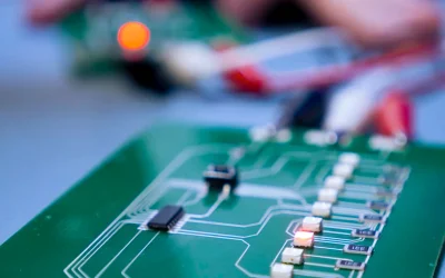
Explore how first-principles engineering and human judgment shape reliable high-voltage IC design, from yield thinking to long-term system lifetime and root-cause discipline.
Be the first to know.
Get our printed electronics weekly email digest.
Tagged with
Printed Electronics
ORGANIZATIONS. SHAPING THE INDUSTRY.
Latest Posts

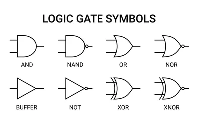
This article provides a detailed examination of logic gate symbols, truth tables, and transistor level implementations, with practical insights for digital design and hardware professionals.

Discover how the new PMIC by Nordic revolutionizes low power design with ultra low ship mode current, seamless activation, and smarter battery management for next generation connected devices.

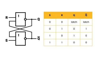
This article explores the basics of SR Latch, covering its fundamental principles and implementation using NOR and NAND gates, metastability and race conditions, illustration of gated variants and real world applications such as switch debouncing and integrated latch ICs.
Learn how to fast-track your PCB development in-house using additive, subtractive and hybrid methods. Discover how modern tools empower engineers to prototype boards faster, iterate smarter, and bring products to market with fewer delays.


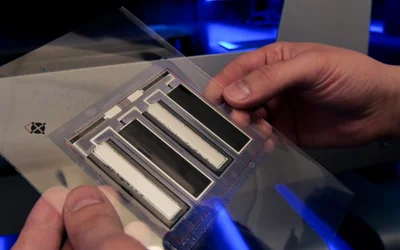
How Voltera's NOVA materials dispensing system can empower defense and military organizations to develop cutting-edge wearable devices for optimal physical and cognitive performance in the field.

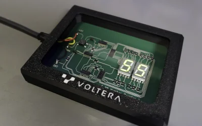
A decimal counter is a digital circuit that cycles through zero to nine using logic components. It is essential in clocks and timers. Making a decimal counter using seven-segment displays offers great opportunities for students to learn sequential logic, clock signals, and circuit integration.
Everything you need to know about choosing the right solder paste when printing electronics, from composition and function to particle size and application.
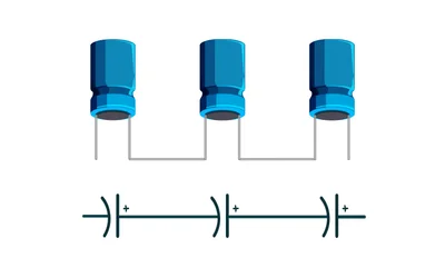
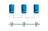
This detailed guide explains the theory behind the capacitors in series, demonstrates how to calculate equivalent capacitance and voltage distribution, and highlights best practices for designing robust, high-voltage electronic systems.
This technical article explains how a transistor as a switch operates. It covers theoretical foundations, bipolar and MOSFET operating regions, practical design calculations, and real world applications.


Explore how Direct Ink Writing (DIW) and Voltera's NOVA system are revolutionizing electronics prototyping—enabling flexible, stretchable, and large-area electronics for next-gen applications in healthcare, consumer tech, and automotive industries.

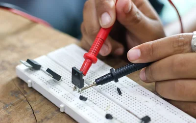
Learn the step-by-step process of testing MOSFET transistors using a digital multimeter and simple circuits. This comprehensive guide covers MOSFET fundamentals, diagnostic techniques, and practical tips for engineers and electronics students.

Flexible printed batteries, highly customizable in size and shape, are the future. Learn more about the technologies enabling these innovative energy storage devices and their latest use cases.


Watch the webinar on sustainable PCB manufacturing hosted by Voltera and Jiva Materials.


Hamamatsu Photonics laser sintering solutions offer greater energy efficiency, scalability, and material versatility for printed electronics.