Featured
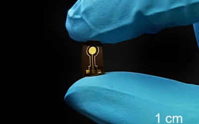
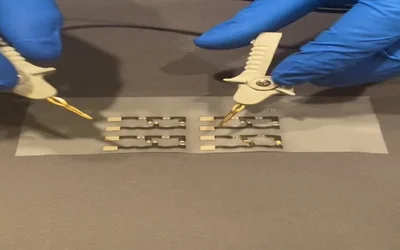
International team develops device for continuous, wireless nitric oxide monitoring

This guide is written for engineers and technical teams building connected devices who need clear, field-ready guidance without getting lost in standards documentation.
PCB Trace Width Calculator
International team develops device for continuous, wireless nitric oxide monitoring
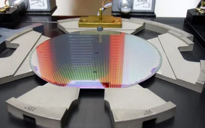
Chips and wafers are the integral components of a semiconductor device. Find out the differences between chip wafers and chips and understand their role in semiconductor manufacturing.
Solder flux has a large impact on final product quality. This article reviews how to use flux during soldering and how to decide on the right technology options for your project.
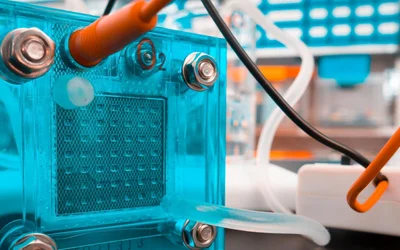
A PEM fuel cell converts hydrogen and oxygen into electricity at around 80 degrees C, with water and heat as the only products. This guide covers electrochemistry, layer materials, efficiency limits, and cost and durability to help you understand the practical applications of this technology.
27 minutes read.
13 minutes read.
21 minutes read.
40 minutes read.
17 minutes read.

Electronics
Mouser Electronics is a worldwide leading authorized distributor of semiconductors and electronic components.
219 Posts
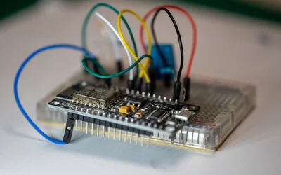
This article explains the ESP8266 pinout, covering GPIO mapping, boot-strapping pins, safe-to-use pins, flash connections, ADC limits, deep-sleep functions, and NodeMCU and D1 mini pin labels.
Learn how a Hall Effect Current Sensor works, including principles, topologies, specifications, comparisons and engineering applications.
A guide covering the full radio-frequency design workflow, starting from setting specifications and choosing topologies to matching, simulation, layout, and verification, to help antenna engineers.
This article presents a detailed technical exploration of SiC MOSFET devices, covering material physics, device structure, switching behavior, and practical design considerations for high-efficiency power electronics systems.
One year after unveiling a first-of-its-kind 'microwave brain' microchip capable of computing on ultrafast data and wireless signals, researchers from the Cornell Duffield College of Engineering have shown how the chip can encode information into its own language.
Ultra-efficient chip design enables extremely strong cryptography algorithms to run on energy-constrained edge devices.
Researchers at ETH Zurich have now developed chip technology that enables verification of the authenticity of sensor data, including images or videos.
Rethinking Supply Chain Security for Multi-Decade Industrial Lifecycles
International team develops device for continuous, wireless nitric oxide monitoring

3 minutes read
Chips and wafers are the integral components of a semiconductor device. Find out the differences between chip wafers and chips and understand their role in semiconductor manufacturing.
Solder flux has a large impact on final product quality. This article reviews how to use flux during soldering and how to decide on the right technology options for your project.

4 minutes read
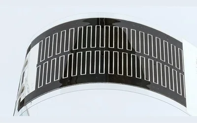
Sometimes manufacturers would like to install heating in objects that are difficult to heat. The armrest of your car. Your sporty winter coat. Bags for food delivery. Sleeping bags. etc This has been difficult to achieve until now. Read more about printed heater technology

2 minutes read
Printed Circuit Board Vertical Interconnect Access (PCB VIAs) are small plated holes that create electrical connections between different circuit board layers. This article delves into the various types, functions, and best practices of PCB VIAs to help you optimize your PCB design.
In the Providentia++ project, researchers at the Technical University of Munich (TUM) have worked with industry partners to develop a technology to complement the vehicle perspective based on onboard sensor input with a bird’s-eye view of traffic conditions. This improves road safety – also for autonomous driving.
Wearable electronic textiles are a demanding environment for reliable interconnects – the ability to function with movement and survive multiple cleanings and reuse. Good adhesion is particularly challenging in these wearable and conformable electronics applications. While solders provide the most conductive electrical connection, they are rigid and require not only the addition of an underfill adhesive but usually a post bond encapsulation. This Anisotropic Conductive Epoxy, provides reliable interconnections between electronic components and circuitry on textiles with excellent structural bonding, without encapsulation, even under repeated stretching and washings. This technology has been shown as a scalable assembly process for e-Textile manufacturing in an SMT line.
5 minutes read
Wafer thinning is a part of the semiconductor manufacturing process. It is essentially grinding off the backside of the wafers to control their thickness and is useful for the production of ultra-thin wafers. These flattened wafers are used to effect stacked and high-density packaging in compact or microelectronic devices. This article discusses the meaning of wafer thinning, along with its various techniques and significance.
Cost of production has been a major barrier despite the fact that Cu raw material prices are far lower than Ag. This is because this large raw material cost difference does not often get translated into equally large nanoparticle dispersion or ink costs. Can this be overcome?
In general, silicone based conductive pastes are rare and the versions with AgCl fillers- needed for many medical wearable applications- are even rarer!
Warp knitting is an excellent candidate. It combines weaving and weft knitting, allowing the warp knitted fabrics to have the stability of woven fabrics and the elasticity of knitted ones.
Conformal EMI shielding is a megatrend on its way to become ubiquitous in electronics. The incumbent process is based on sputtering a tri-layer structure consisting of SUS on the EMC of the package. In these slides, you can see performance analysis and detailed cost analysis/projections.
2 minutes read
This article describes the TAeTTOOz printable battery technology developed by Evonik and acquired by InnovationLab for upscaling and mass production. In this article, you can learn about the operating principles, the key working characteristics, the material set, production techniques, and emerging applications of this technology
7 minutes read
Why can microLED technology can help narrow the energy gap in electronic devices? The first slide shows the battery gap- Ahmed (Intel) has collected data by year showing that power demand of phones far exceeds the power supply level of batteries, creating a "battery gap" which ...
The new approach moves energy efficiently and could reduce energy losses converting light into electricity.

3 minutes read