Featured
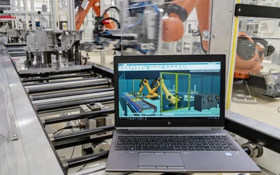
A brief guide to creating a digital twin with LoRaWAN® sensors.

This guide is written for engineers and technical teams building connected devices who need clear, field-ready guidance without getting lost in standards documentation.
PCB Trace Width Calculator
A brief guide to creating a digital twin with LoRaWAN® sensors.
At the DVT stage, your design is not yet ready for manufacturing. All certifications, qualifications, and specification requirements get tested now.
PCB layers are the copper layers within a printed circuit board, laminated between or onto layers of conductive material. These layers are stacked to enhance the functionality of electronic devices. This article explores the concept of PCB layering, the various types of layers, and their benefits.
A PEM fuel cell converts hydrogen and oxygen into electricity at around 80 degrees C, with water and heat as the only products. This guide covers electrochemistry, layer materials, efficiency limits, and cost and durability to help you understand the practical applications of this technology.
27 minutes read.
13 minutes read.
21 minutes read.
40 minutes read.
17 minutes read.

Electronics
Mouser Electronics is a worldwide leading authorized distributor of semiconductors and electronic components.
219 Posts
This article explains the ESP8266 pinout, covering GPIO mapping, boot-strapping pins, safe-to-use pins, flash connections, ADC limits, deep-sleep functions, and NodeMCU and D1 mini pin labels.
Learn how a Hall Effect Current Sensor works, including principles, topologies, specifications, comparisons and engineering applications.
A guide covering the full radio-frequency design workflow, starting from setting specifications and choosing topologies to matching, simulation, layout, and verification, to help antenna engineers.
This article presents a detailed technical exploration of SiC MOSFET devices, covering material physics, device structure, switching behavior, and practical design considerations for high-efficiency power electronics systems.
One year after unveiling a first-of-its-kind 'microwave brain' microchip capable of computing on ultrafast data and wireless signals, researchers from the Cornell Duffield College of Engineering have shown how the chip can encode information into its own language.
Ultra-efficient chip design enables extremely strong cryptography algorithms to run on energy-constrained edge devices.
Researchers at ETH Zurich have now developed chip technology that enables verification of the authenticity of sensor data, including images or videos.
Rethinking Supply Chain Security for Multi-Decade Industrial Lifecycles
A brief guide to creating a digital twin with LoRaWAN® sensors.
At the DVT stage, your design is not yet ready for manufacturing. All certifications, qualifications, and specification requirements get tested now.

3 minutes read
PCB layers are the copper layers within a printed circuit board, laminated between or onto layers of conductive material. These layers are stacked to enhance the functionality of electronic devices. This article explores the concept of PCB layering, the various types of layers, and their benefits.
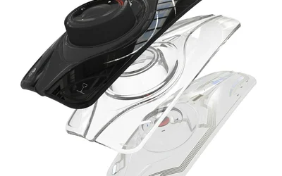
In this article, we look at how Super Low power Wi-Fi and Bluetooth LE enable smart locks to be more agile and reliable by demonstrating these features with a case study from Renesas.
The EVT Stage implements the design in its form, fit, and function to better inform stakeholders of your production intent. Don't rush this important milestone.
3 minutes read
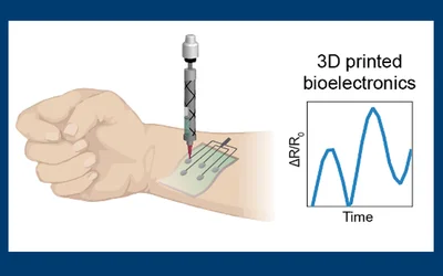
Flexible electronics have enabled the design of sensors, actuators, microfluidics and electronics on flexible, conformal and/or stretchable sublayers for wearable, implantable or ingestible applications.
Article #3 of the Enabling IoT Series. This article looks at how Time of Flight (ToF) sensors are used for this purpose and are changing the way we can interact with VR, and other video technologies.
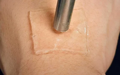
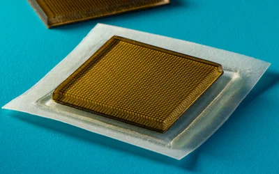
Canadian researchers have discovered that they can stick hydrogel plasters to the skin very effectively using ultrasound. Outi Supponen has now explained the underlying mechanism: imploding bubbles that form within the adhesive located between the plaster and the skin anchor the one on the other.

2 minutes read
Open and honest communication is crucial to a successful design. Product and engineering decision-makers need to work in sync.
4 minutes read
Phosphors or QDs for color conversion in LCD and microLED ? Which will win? This is an evolving technology space to watch. Here, it is shown that phosphor technology is evolving, enabling not just red but also green narrowband color conversation with small particle sizes compatible with microLEDs

2 minutes read
Molecular particle free inks can offer extreme formability and stretchability, allowing the design and production of 3D shaped and/or in-mold electronics parts with extreme curvatures and complex shapes.
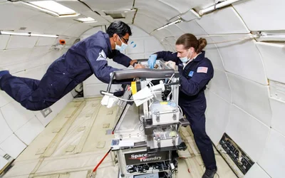
As NASA prepares to send astronauts back to the Moon to live and explore, capabilities for space-based manufacturing of sensors, circuits, and other electronics will become increasingly critical. Recent microgravity flights have helped to advance cutting-edge methods for 3D printing of electronics

4 minutes read
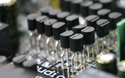
This article delves into the specifics of NPN and PNP transistors, their working principles, applications, comparisons, and factors to consider when choosing between them.
In this episode, we talk about how researchers are developing a sticker that can conduct ultrasound tests along with a machine learning powered robotic solution for choosing chemical proteins when developing new drugs and biofuels or recycling plastics.

The rigid, flex and rigid-flex PCBs are all types of printed circuit boards. The rigid PCB is the traditional board and the base from which the other two variations came about, in response to industry and market needs. Flex PCBs introduced versatility to PCB fabrication and rigid-flex combines both for increased performance. Learn more about these board types, their benefits, disadvantages, and applications in this article.