Engineering Designs For Reduced Costs
The best designs must consider all available opportunities to reduce costs at the outset. We give some common sense guidelines that can make a difference in your bottom line.
22 Jul, 2022. 7 minutes read
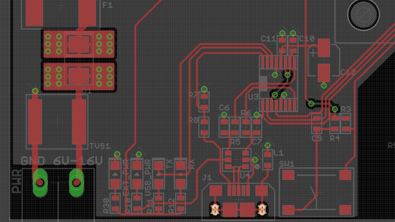
Consider the minimum number of signal and ground layers in your PCBA
This article was first published on
macrofab.comEngineering Designs for Reduced Costs
The competitive landscape for electronics systems dictates that new engineering designs must be differentiated in performance from other similar systems in the market. However, as technology and manufacturing capabilities continue to advance unabated, even a unique static design will eventually face cost pressures. The best designs must consider all the available opportunities to reduce costs at the onset. In order to reduce the total PCB system costs, several key design decisions need to be considered in advance of the first build. These items address the areas that can be controlled by the design team.
Surface Mount vs. Plated Through-Hole
Surface mount technology (SMT) for PCB assembly is generally the lowest cost and minimum hassle process for manufacturing new engineering designs. Where possible, reduce or remove all plated through-hole (PTH) components as they require more costly manual assembly work. Some ruggedized external connectors may only be offered in through-hole options. Consider surface mount connectors with additional fasteners if needed.
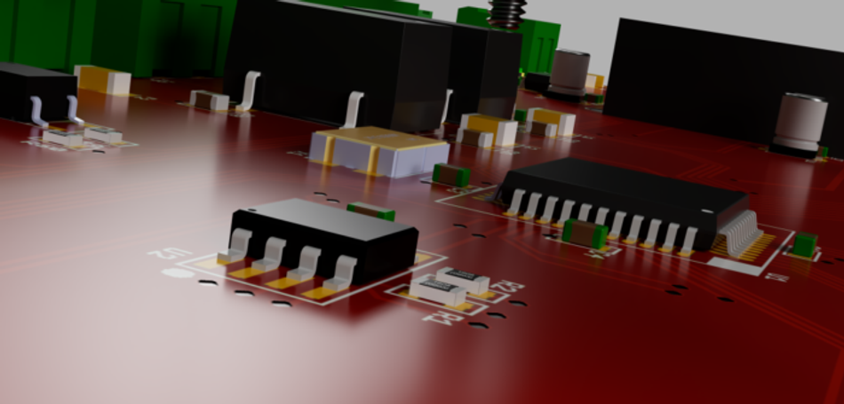
PTH components are generally stronger and more rugged than SMT components. This makes them ideal for connectors. In the cases where PTH components are mandatory, discuss ‘Paste in Hole’ (PIH) technology with your CM. This is the process of screening solder paste into and around plated through-holes on a PCB. Then, the leads of the through-hole components are placed into these prepared through-holes. The PCBs are run through only a single reflow soldering process, thus terminating both through-hole and SMT components at one time. PIH makes it easier, faster and cheaper to process double-sided boards.
PIH requires two prerequisites of the design. First, the insulator material of the component must be capable of withstanding lead or lead-free reflow temperatures. Check the datasheet of the components in question to verify this information. Second, the vertical and horizontal clearance around the leads must be large enough to allow an adequate volume of printed solder paste. This space is required to allow an unobstructed transfer of molten paste from the PCB surface into the plated through holes.
For relatively low component count designs, use a single-sided PCB SMT when possible. While this may apply only to a limited number of systems, it can dramatically reduce the assembly complexity. The simpler the assembly process, the better and lower the costs. Re-work of assembly due to unnecessary complexity and component damage delays throughput and increases costs.
Layout
The size of the PCB will directly impact its cost as this will dictate the number of systems per panel. The layout should be minimized as much as possible in size while also considering the minimum number of signal and ground layers within the PCB. Although a circuit block may be re-used from a previous design, its use within a different system may require a new layout due to its complementary functions.

Blind vias, ones that are buried within the PCB, are often used to minimize the spatial impact on the top and bottom planes. However, work with your CM to understand the fabrication capabilities of blind vias and their impact on cost. Your CM can also help you understand the maximum array size for PCB count per panel. This will maximize the number of boards built at one time.
Scrutinize Each BOM Component
Each component within a bill of materials (BOM) should provide unique value to the system. To test for this case, consider if the system would operate improperly, poorly, or even fail entirely if a component was missing. For most of the components, this would obviously be true. However, redundant parallel bypass capacitors, for example, may often sneak into a design at every active component supply pin.
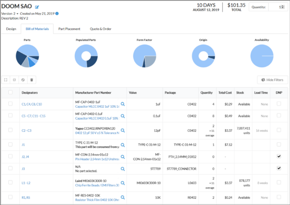
Sometimes, a designer may simply re-use a legacy design block since ‘it has always been done this way.' However, unless the manufacturer’s datasheet calls out for extreme bypassing at every supply pin, there may be some opportunity for bypass capacitor relief. Also, vet all pull-up and pull-down resistors on signal I/O to determine if indeed these are needed within the design. If the active component already provides an internal pull-up or pull-down, then this external resistor may be redundant.
Component Performance Drives Cost
Component manufacturers segment and market their products just like any other industry. For cost reasons, it is important to review all the advertised features of a component. Only purchase those performance features that are needed. Draw the line at ‘better than required’ features that only add cost with no added value to the system:
- Tolerance – Passive component vendors segment their products by offering several tolerance ranges of capacitors, resistors, inductors, and others such as 1%, 5%, 10%, and 20%. This helps them sell the full capacity of their factory for the highest price a customer is willing to pay for the tolerance accuracy achieved by their manufacturing. Again, to test the relevance of system tolerance, consider if your system would operate improperly, poorly or even fail entirely if a component was out of tolerance. If not, consider widening the tolerance for a lower-priced passive component.
- Power requirements and size – Passive components are rated on their maximum power consumption, such as ¼ watt resistors. Evaluate the maximum required power requirement for each passive component and only include required criteria on the BOM. This also typically drives to minimum-sized components.
- Active circuit performance – The best systems may require the highest performing active components. When clock rate, switching speed, signal-to-noise ratio, or high gain drive the differentiation, then the highest performance semiconductors have no substitute. However, for those areas of the application where that is not the case, ensure that the system is not ‘over designed’ using higher performance integrated circuits than needed as this will only drive additional cost. Review legacy circuit blocks that may be re-used for simplicity, but result in higher performance than required by the system.
- Memory Size – Although memory is nearly always offered in sizes of 2n bits, empty unused memory offers no additional value. Condense firmware or computational memory as much as possible and only use the minimum memory size that the system requires.
- Temperature grade – Component vendors often differentiate their products across several temperature grades to segment their market. Consumer (0-70C), Industrial (-25–85C) and Automotive (-40-105C) garner successively higher pricing depending upon the range. Ensure that the temperature grade of the components within your BOM meets, and does not exceed, your system application requirements. Reduce the temperature grade for components when warranted.
- Vendor selection – There may be equivalent or pin-compatible competitive offerings that are lower cost. Consider all applicable component vendors.
For any custom component within the system, determine if this can be sourced through multiple vendors with competitive quotes. A sole-sourced custom component from a single supplier will come at a premium cost. If at all possible, engage two or more suppliers with interchangeable parts that each wins some portion of your production volume.
Volume and Procurement
Consider working closely with the logistics planner for the system, either internally or with your turn-key CM, to procure components in larger quantities. Once your system is stable in production with a mature run-rate, larger volume purchases may make sense to reduce the component pricing over the longer term. As a general rule of thumb, component pricing typically continues to be inversely proportional to volume until quantities exceed >100,000-250,000. At some point beyond this volume, the pricing establishes a floor and additional volume no longer drives appreciably lower component costs.
Review component costs across as many distributors as possible to get the best pricing. Alternately, a turn-key CM has access to a broad choice of distributors and can aggregate their orders for better economies of scale. In some cases of large volume, buying particular high-value components directly from the component manufacturer may be an option to bypass a distributor mark-up. A component vendor will let you know what volume or dollar value will qualify to be a direct OEM account. Consolidate the variety of components by using the same values of R or C across the BOM where possible. This will drive higher volumes of fewer discrete values.
As many engineering designs go through several iterations of test and debugging before they are ready for final production, it is possible that there are embedded test mode circuits within the first system design that are no longer valuable in production. Unless a test points or debug circuit is needed to observe a behavior during or after production, consider removing test modes or non-essential functions for system production versions. This may include replacing zero ohm resistor test points with a new trace or solder. Additionally, the final PCB layout design should be reduced in size to remove any circuit debug area.
Packaging
A design team may be indifferent to the component packaging, other than pricing. However, it may create excess complexity for the assembly within manufacturing. Work with your CM to understand how the component packaging form can reduce costs due to the ease of use on their pick-and-place machinery. A non-standard packaging may require more handling or push the CM to use a less efficient or costlier older piece of equipment.
Although tape and reel are often the most common packaging, some older vintage analog components may still only be offered in a tube format. Larger and more sophisticated semiconductors may also only be offered in trays. Understand the impact on your manufacturing facility of these design and ordering tradeoffs.
Conclusion
Before handing over new engineering designs to a CM for production, consider all avenues for cost reduction during the design phase. While PCB layout is typically the first to be considered for lower costs, there are also many options to review for the BOM and its procurement. There may be some tradeoffs for cost vs. performance. These are the proper discussions to have with the design team to ensure that the system is not over-designed, but optimized for what the market will support. This will allow maximum flexibility for efficiencies during the course of manufacturing. For more information, view Designs for Reduced Costs – Supply Chain.