Non-Inverting Amplifier Design: Op-Amp Theory, Bandwidth, Noise, and Practical Implementation
A non-inverting amplifier is an op-amp configuration that delivers in-phase voltage gain with high input impedance. This article explains its theory, schematic symbols, gain calculation, bandwidth limits, noise, stability trade-offs, and real-world design practices.

02 Feb, 2026. 17 minutes read
Key Takeaways
A non-inverting amplifier is an op-amp configuration that provides in-phase amplification with high input impedance, making it well-suited for buffering, signal conditioning, and sensor interfaces where loading the source must be avoided.
The feedback network defines the closed-loop voltage gain and can be calculated as:
Av = 1 + (Rf / R2)
In practice, the gain accuracy is influenced by finite open-loop gain, resistor tolerances, and temperature drift.Bandwidth is limited by the op-amp’s gain-bandwidth product (GBW). As voltage gain increases, usable bandwidth decreases according to:
Bandwidth ≈ GBW / Av
Capacitive loading and parasitic capacitances can further reduce stability at high frequencies.Large-signal performance is constrained by slew rate, not bandwidth alone. Even unity-gain-stable op-amps can introduce distortion when fast input signals demand output voltage changes faster than the specified slew rate.
Precision is ultimately limited by non-ideal effects such as input bias currents, voltage noise, common-mode rejection, and power-supply rejection. Careful resistor selection, layout discipline, and compensation techniques are required for stable, low-noise operation.
Introduction
Operational amplifiers (op-amps) are among the most fundamental building blocks in analog electronics, forming the backbone of countless signal conditioning, amplification, and control applications. From audio circuits and sensor interfaces to industrial control systems and power management designs, op-amps enable engineers to manipulate voltage signals with precision and predictability.
One of the most widely used op-amp configurations is the non-inverting amplifier. Valued for its high input impedance, stable gain characteristics, and straightforward implementation, this configuration allows designers to amplify a signal without altering its phase. As a result, it is commonly employed where signal integrity must be preserved—particularly when interfacing with high-impedance sources such as sensors, transducers, and reference voltages.
Understanding how a non-inverting amplifier works goes beyond knowing its gain formula. Effective design requires familiarity with feedback behavior, bandwidth limitations, slew rate constraints, and the non-ideal characteristics of real-world op-amps. Equally important is the ability to interpret circuit schematics accurately. In this context, electronic component symbols serve as the universal language of electronics, allowing engineers across disciplines and geographies to communicate complex circuit behavior clearly and consistently.
Understanding the Non-Inverting Amplifier Configuration
The non-inverting amplifier is a foundational op-amp topology that provides voltage gain without inverting the input signal. Its defining feature is that the input voltage (Vin) is applied directly to the non-inverting terminal (+). In contrast, a feedback network between the output (Vout) and the inverting terminal (−) determines the closed-loop gain. This configuration ensures that the output remains in phase with the input while maintaining high input impedance, a key requirement for interfacing with sensitive or high-impedance sources.
Basic Circuit Topology
A typical non-inverting amplifier uses two resistors to form a feedback voltage divider:
Rf: the resistor from the output to the inverting input
R2: the resistor from the inverting input to ground
The inverting input forms a virtual ground, meaning the voltage at this node is forced by negative feedback to match Vin (assuming the op-amp operates within its linear region).
Closed-loop voltage gain formula:
Av = Vout / Vin = 1 + (Rf / R2)
Example: Selecting Rf = 9 kΩ and R2 = 1 kΩ produces a gain of Av = 1 + 9k/1k = 10.
Key Characteristics
High Input Impedance
Because the input is applied to the op-amp’s non-inverting terminal, the input impedance is essentially that of the op-amp itself—typically in the megaohm to gigaohm range for modern devices. This minimizes loading on preceding stages, making the topology ideal for sensors, thermocouples, and high-impedance voltage references.Low Output Impedance
The closed-loop configuration drives the output with very low impedance (tens of milliohms in many modern op-amps), allowing the amplifier to deliver current to loads without significant voltage drop.Phase Relationship
The output signal is in phase with the input, which distinguishes the non-inverting amplifier from its inverting counterpart. This characteristic is critical in applications where phase integrity is essential, such as differential measurement systems or multi-stage amplification.Special Case – Voltage Follower (Unity Gain Buffer)
Setting Rf = 0 Ω and removing R2 converts the non-inverting amplifier into a voltage follower. In this configuration: Av = 1. Vout = Vin
The voltage follower preserves signal amplitude while providing extremely high input impedance and low output impedance, effectively isolating a high-impedance source from a load.
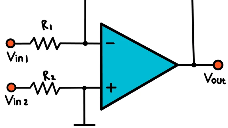
Comparison with Inverting Amplifier
The non-inverting amplifier differs fundamentally from the inverting configuration. In an inverting amplifier, the input signal is applied through a resistor (Rin) to the inverting terminal (−), while the non-inverting terminal (+) is grounded. The closed-loop gain is:
Non-inverting amplifiers maintain positive gain, high input impedance, and better common-mode rejection, making them preferable in sensor interfacing and precision applications.
Av = -Rf / Rin
The negative sign indicates a 180° phase inversion between the input and output. Because the input is applied through (Rin), the input impedance equals Rin, which can load the source if not carefully chosen.
In contrast, the non-inverting amplifier applies the input to the non-inverting terminal (+), resulting in positive gain and high input impedance, typically in the mega-ohm to giga-ohm range. These characteristics make the non-inverting amplifier ideal for buffering high-impedance sources, sensor interfaces, and signal conditioning.
Non-inverting op-amps also typically exhibit higher common-mode rejection (CMRR) and lower noise compared with inverting configurations, improving performance in precision applications.
Table 1 – Key Formulas and Characteristics
Configuration | Voltage Gain Av | Phase Relationship | Input Impedance | Output Impedance |
Non-inverting amplifier | Av = 1 + Rf / R2 | Output in phase with input | High (≈ op-amp input impedance) | Low (≈ op-amp output impedance) |
Voltage follower (unity gain) | Av = 1 | Output follows input | Extremely high | Very low |
Inverting amplifier | Av = -Rf / Rin | Output 180° out of phase | Rin | Low |
These relationships provide a clear framework for component selection and help engineers anticipate performance differences when choosing between non-inverting and inverting topologies.
Recommended reading: Inverting vs Non-Inverting Op Amp: Complete Design Guide & Best Practices 2025
Practical Notes
The feedback resistors not only set the gain but also influence the noise and offset. Larger resistances increase thermal (Johnson) noise and bias-current-induced offsets, while smaller resistances draw more current from the op-amp output. Designers typically select resistor values between 1 kΩ and 100 kΩ to balance noise, power, and accuracy.
Capacitive loading on the output can introduce oscillations or peaking; placing a small series resistor (20–50 Ω) or an RC snubber across the feedback resistor improves stability.
Understanding this configuration is essential before interpreting schematic symbols, as the amplifier’s behavior is defined by both the op-amp and the surrounding components.
Electronic Component Symbols: The Universal Language of Electronics
Circuit schematics are more than drawings—they are the universal language of electronics, enabling engineers across the globe to understand, design, and communicate complex systems without ambiguity. Before diving into design and analysis, it’s essential to interpret these symbols correctly, especially in precision applications like non-inverting amplifier circuits.
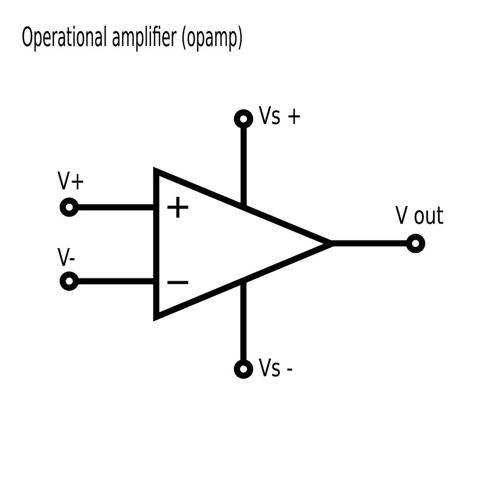
Op-Amp Symbol
In schematics, the operational amplifier is typically represented as a triangle with three terminals:
Non-inverting input (+): receives Vin in a non-inverting amplifier
Inverting input (−): connected to the feedback network
Output: drives Vout to the load
Some symbols also indicate power supply pins (V+ and V−), though these are often omitted in simplified diagrams. Recognizing the op-amp symbol is crucial for distinguishing input polarity, which directly affects signal phase and gain.
Resistors
Resistors (Rf and R2 in a non-inverting amplifier) are represented by either zigzag lines (American standard) or rectangles (IEC/European standard). Their values are usually annotated next to the symbol. In feedback networks, the placement of resistors relative to the op-amp symbol clearly shows the gain-determining path, allowing engineers to quickly calculate the closed-loop gain:
Av = 1 + (Rf / R2)
Capacitors
Capacitors appear as parallel lines, sometimes with one curved line for polarized electrolytics. In amplifier schematics, capacitors are often used for:
Decoupling: stabilizing power supply rails near the op-amp
Feedback compensation: controlling frequency response and preventing oscillation
Recognizing capacitor placement in the schematic helps identify stability and bandwidth considerations.
Nodes and Connections
Dots or junctions indicate electrical connections. Lines without a dot imply no connection, a detail often overlooked but critical in high-density schematics. Misinterpreting connections can lead to errors in gain calculations or instability in real-world prototypes.
Voltage Sources
Symbols for voltage sources (batteries or DC rails) define the supply voltages for the op-amp. Proper interpretation ensures that the designer accounts for rail-to-rail output limitations, PSRR, and input common-mode voltage range, all vital for reliable operation.
Example: Non-Inverting Amplifier Schematic
A typical schematic for a non-inverting amplifier will include:
Triangle symbol for the op-amp
Rf connecting the output to the inverting input (−)
R2 from the inverting input (−) to ground
Vin connected to the non-inverting input (+)
Vout at the op-amp output
Optional decoupling capacitors near the power pins
Understanding these symbols allows engineers to translate the theoretical configuration into a physical design, verify component placement, and identify potential pitfalls like parasitic capacitances or long feedback traces that can cause oscillation.
Why Symbols Matter
For engineers, proficiency in reading component symbols is just as important as understanding equations. Schematics are a compact representation of circuit function, allowing rapid diagnosis, troubleshooting, and collaboration. Mastery of this “language” ensures that complex topologies like non-inverting amplifiers can be implemented accurately, efficiently, and consistently, bridging the gap between theory and practical hardware design.
Recommended reading: How to Read Electrical Schematics: A Comprehensive Guide for Engineers
Calculating Gain and Closed-Loop Behavior
The non-inverting amplifier achieves a predictable gain using a feedback resistor network. The input voltage Vin is applied to the non-inverting terminal (+), and the feedback resistor Rf connects the output to the inverting terminal (−), which is also connected to ground through R2.
Closed-Loop Gain Formula
Assuming an ideal op-amp (infinite open-loop gain, zero input current), the closed-loop voltage gain is:
Av = Vout / Vin = 1 + Rf / R2
Rf = feedback resistor between output and inverting input
R2 = resistor from inverting input to ground
Example:
If Rf = 9 kΩ and R2 = 1 kΩ, the gain is:
Av = 1 + 9000 / 1000 = 10
Input and Output Impedance
Input impedance (Zin) is extremely high because the signal is applied to the non-inverting input:
Zin ≈ op-amp input impedance ≈ mega-ohms to giga-ohms
This ensures minimal loading on the preceding stage, making non-inverting amplifiers ideal for sensor outputs and high-impedance sources.
Output impedance (Zout) is very low when operating in closed loop:
Zout ≈ op-amp output impedance ≈ tens of milliohms
Low output impedance allows the amplifier to drive downstream circuits with minimal voltage drop.
Special Case: Voltage Follower (Unity-Gain Buffer)
When the feedback resistor Rf = 0 Ω and R2 is removed (open-circuit), the non-inverting amplifier becomes a voltage follower:
Av = 1
Vout = Vin
Input impedance: extremely high
Output impedance: very low
This configuration is often used to buffer high-impedance sources before connecting to low-impedance loads or ADCs.
Practical Considerations
Resistor Tolerances: Use precision resistors (0.1% or better) to maintain accurate gain.
Bias Currents: Match resistances seen by both op-amp inputs to minimize offset voltage caused by input bias currents.
Load Effects: For capacitive loads, a small series resistor at the output improves stability.
Frequency Response and Slew Rate
In practical applications, the frequency behavior of a non-inverting amplifier is as important as its DC gain. Understanding gain-bandwidth trade-offs and slew rate limitations ensures the amplifier performs reliably across the intended signal range.
Open-Loop Gain and Gain-Bandwidth Product (GBW)
Real op-amps have a finite open-loop gain (Aol) that decreases with frequency due to internal compensation capacitors. A typical open-loop gain vs. frequency plot shows a single-pole roll-off at −20 dB/decade.
For a non-inverting amplifier, the closed-loop bandwidth is determined by the gain-bandwidth product (GBW):
GBW = Av * f3dB
Where:
Av = closed-loop gain (1 + Rf / R2)
f3dB = bandwidth at which the gain drops by 3 dB
Example:
If an op-amp has GBW = 1 MHz and you configure a gain Av = 10:
f3dB ≈ GBW / Av = 1 MHz / 10 = 100 kHz
This relationship highlights the trade-off between gain and bandwidth—higher gain reduces the available bandwidth.
Noise Gain and Stability
The noise gain of a non-inverting amplifier equals its signal gain:
Noise Gain = 1 + Rf / R2
Phase margin decreases as noise gain increases, which can cause oscillations in high-gain configurations.
Current-feedback op-amps may have a minimum stable gain greater than unity; datasheets specify recommended feedback resistor values for stability.
For capacitive loads, adding a small series resistor (20–50 Ω) at the output or an RC snubber across the feedback resistor improves stability.
Slew Rate and Rise Time
The slew rate (SR) defines the maximum rate at which the output voltage can change:
SR = dVout / dt [V/µs]
If the input changes faster than the op-amp can respond, slew-induced distortion occurs.
Estimating rise time for a step input:
Tr ≈ 0.8 * ΔVout / SR
Example:
Step: ΔVout = 5 V
Op-amp: μA741, SR = 0.5 V/µs
Tr ≈ 0.8 * 5 / 0.5 ≈ 8 µs
Modern high-speed op-amps, like the LT1817, offer:
SR = 1500 V/µs
GBW = 220 MHz
Enabling video, RF, and high-speed buffering applications.
Precision Considerations: Noise and Bias Currents
Even the most carefully designed non-inverting amplifier can face challenges from real-world imperfections. Understanding these effects is key to maintaining accuracy, stability, and high input impedance in practical circuits.
Input Offset and Bias Current Compensation
Every op-amp has a small input offset voltage—a tiny difference between the terminals that can cause the output to drift even when no signal is applied. Input bias currents, which are tiny currents flowing into the op-amp’s inputs, can interact with resistors in the feedback network and create additional offsets.
To reduce these errors, engineers use symmetrical resistor networks and sometimes add a resistor in series with the non-inverting input that matches the combined resistance of the feedback resistors. This simple adjustment balances the voltage drops caused by bias currents and keeps the output voltage as close as possible to what the design intends.
Resistor Values and Noise Trade-Offs
Resistors in a non-inverting op-amp circuit are not just passive components—they affect thermal noise and precision.
Lower resistor values reduce noise but increase current draw and can overload the input signal.
Higher resistor values minimize loading but can increase noise and sensitivity to bias currents.
For most voltage-feedback non-inverting amplifiers, using feedback resistors between 1 kΩ and 10 kΩ is a good balance, offering stable gain without compromising the high input impedance or adding excessive noise.
Op-Amp Noise Sources
All op-amps generate some noise, which can limit precision in sensitive applications like sensor amplification. There are two main types:
Voltage noise – a small, random fluctuation at the input.
Current noise – tiny currents flowing into the op-amp inputs that create additional voltage fluctuations when interacting with resistors.
By carefully selecting low-noise op-amps and appropriate resistor values, designers can minimize total noise and preserve the signal quality.
Recommended reading: Difference Amplifier: Theory, Design, and Applications for Engineers
Instrumentation Amplifiers
When ultimate precision is required, engineers turn to instrumentation amplifiers. These are essentially multi-stage non-inverting amplifiers designed to amplify very small signals while maintaining high input impedance and excellent common-mode rejection (CMRR).
The first stage buffers the input signal to prevent loading.
The second stage provides differential gain, ensuring small differences are amplified without amplifying noise or interference.
Modern examples like the AD620 offer CMRR ≥ 100 dB, input bias currents < 1 nA, and extremely low voltage noise (~9 nV/√Hz), making them perfect for weigh scales, ECG circuits, strain gauges, and other precision measurements.
Common‑Mode and Power Supply Rejection
Non‑inverting amplifiers are often used in precision applications, so understanding how they reject unwanted signals is essential. Two critical parameters govern this: common‑mode rejection ratio (CMRR) and power supply rejection ratio (PSRR).
Common‑Mode Rejection Ratio (CMRR)
The CMRR quantifies how well an amplifier ignores signals that are common to both input terminals. In other words, it measures the amplifier’s ability to reject interference or noise that appears simultaneously on both the non‑inverting and inverting inputs.
A high CMRR ensures that unwanted voltages, such as electromagnetic interference or voltage offsets from long sensor wires, do not appear in the output signal. Non‑inverting amplifiers benefit from the op‑amp’s internal architecture, which directly applies the input voltage to the positive terminal. However, finite CMRR allows some of this common-mode voltage to leak into the output voltage, especially in high-gain or high-precision circuits.
Modern precision op‑amps, like the AD620, achieve CMRR exceeding 100 dB at gains of 10, making them ideal for sensor signal conditioning and instrumentation amplifiers. When designing non‑inverting circuits, carefully matched feedback resistors and low-tolerance components preserve high CMRR.
Power Supply Rejection Ratio (PSRR)
The PSRR measures how variations in the power supply affect the amplifier’s output voltage. A higher PSRR means the op-amp circuit is less sensitive to supply noise, such as ripple from switching regulators or battery voltage changes.
PSRR is specified in either microvolts per volt (µV/V) or decibels (dB). For instance, an op‑amp with a PSRR of 0.05 µV/V will produce only a 50 nV change in output if the supply voltage changes by 1 V. AC PSRR, however, often decreases at higher frequencies, meaning switching noise can couple into the output signal unless mitigated.
To maximize PSRR in non‑inverting amplifiers:
Place bypass capacitors (typically 0.1 µF ceramic in parallel with 1 µF electrolytic) close to the op-amp power pins.
Use low-noise linear regulators for sensitive analog circuits.
Avoid routing high-frequency digital signals near the analog input terminals.
By carefully selecting op‑amps with high CMRR and PSRR, engineers can design non-inverting amplifier circuits that maintain signal integrity even in electrically noisy environments, making them suitable for precision measurement, data acquisition, and sensor interfacing.
Recommended reading: VSS vs VDD: Understanding Power Rails in Electronic Circuit Design
Design Guidelines and Best Practices
Designing a reliable non‑inverting amplifier involves careful selection of components, layout, and compensation techniques to ensure stable, low-noise, and precise operation. Below are practical guidelines for engineers and electronics students.
Selecting Resistor Values
The closed-loop gain of a non-inverting amplifier is determined by:
Av = 1 + Rf / R2
Resistor choice affects both noise and bias current-induced offset:
Low-value resistors reduce thermal (Johnson) noise and improve high-frequency performance but increase current draw and loading.
High-value resistors reduce loading but increase noise and susceptibility to bias currents.
A good compromise is using resistors between 1 kΩ and 10 kΩ for voltage-feedback op-amps. For current-feedback op-amps, always follow the manufacturer’s recommended feedback resistor to maintain stability.
Bias Current Compensation
To reduce output offset caused by input bias currents, insert a resistor in series with the non-inverting input equal to the parallel combination of Rf and R2:
Rcomp = (Rf * R2) / (Rf + R2)
Using CMOS or JFET input op-amps further minimizes offset because of their picoamp-level input bias currents.
Managing Capacitive Loads and Stability
Capacitive loads can destabilize an amplifier:
Add a series resistor at the output (20–50 Ω) to isolate the load.
For larger loads, use a snubber network (series resistor + capacitor) across Rf to shape the frequency response.
Keep feedback traces short and parallel and minimize parasitic capacitances at the inverting input.
This maintains phase margin, reduces oscillation, and preserves bandwidth.
Layout and Grounding
Proper PCB layout improves signal integrity:
Separate analog and digital grounds, connecting at a single point.
Use a continuous ground plane under the amplifier and feedback network.
Place bypass capacitors (0.1 µF + 1 µF) close to op-amp supply pins.
Keep traces to the inputs short, especially the inverting input node, to reduce noise.
Recommended reading: What Is Ground in a Circuit? Understanding Grounding Concepts and Implementations
Temperature Effects and Drift
Temperature changes affect resistor values and op-amp offsets:
Use low-drift metal-film resistors for feedback.
Choose op-amps with low input offset voltage and minimal temperature coefficient. Example: AD620 has 50 µV max offset and 0.6 µV/°C drift.
Implement calibration or compensation in extreme conditions.
Simulation and Prototyping
Before building hardware:
Simulate frequency response, transient response, and noise using LTspice, TINA-TI, or QSPICE.
Breadboard or prototype, measuring rise time, output signal quality, and bandwidth.
Adjust compensation (series resistors, snubbers) if overshoot or ringing occurs.
Applications of Non‑Inverting Amplifiers
Non‑inverting amplifiers are extremely versatile, forming the foundation of many analog and mixed-signal circuits. Their high input impedance, predictable gain, and phase-preserving behavior make them ideal for a variety of engineering applications. Here’s how they are commonly used:
Voltage Amplification and Level Shifting
Non‑inverting amplifiers boost small signals, such as sensor outputs or microphone voltages, to levels suitable for analog-to-digital converters (ADCs).
The input impedance is high, preventing loading of the source.
Offset voltages can be added at the non-inverting input to shift signals into the ADC’s range.
Example: For a single-supply ADC, applying half the supply voltage to the non-inverting input allows amplification of a bipolar signal without clipping.
Unity-Gain Buffers and Impedance Matching
When a high-impedance source drives a low-impedance load, a voltage follower isolates the stages:
Av = 1
Output follows input exactly.
Input impedance is extremely high; output impedance is very low.
Common uses include buffering high-impedance sensors, driving coaxial cables, or providing stable reference voltages.
Signal Conditioning for Precision Sensors
For sensitive devices such as strain gauges, thermocouples, and photodiodes:
Moderate gain (10–100) ensures signals are amplified without loading.
Low-pass filtering can reduce high-frequency noise and prevent aliasing.
This allows precise measurement in data acquisition and instrumentation systems.
Active Filters and Oscillators
Non‑inverting op-amps are key in active filter circuits:
Low-pass, high-pass, band-pass, and band-stop filters.
Oscillator circuits, such as phase-shift oscillators, use feedback networks to control frequency.
High input impedance prevents reactive components from being loaded, ensuring accurate filter or oscillator performance.
Recommended reading: What Is a Low Pass Filter? Theory, Design & Practical Implementation
Precision References and Voltage Regulators
Non-inverting amplifiers can buffer or scale precision voltage references:
High common-mode rejection and low noise maintain reference accuracy.
In regulator circuits, the amplifier monitors the output voltage and provides an error signal to control loops.
Instrumentation Amplifiers and Data Acquisition
Instrumentation amplifiers are essentially multi-stage non-inverting amplifiers designed for high CMRR and precise differential signal amplification:
First stage gain: 1 + 2*R2/R1
Differential stage gain: R4/R3
Ideal for bridge sensors and industrial transducers.
Example: AD620 provides 100 dB CMRR at a gain of 10, 1 nA max input bias current, and low voltage noise (9 nV/√Hz).
Applications include weigh scales, ECG circuits, and industrial control systems.
Conclusion and Future Outlook
The non-inverting amplifier remains a fundamental building block in analogue and mixed-signal electronics. Its high input impedance, positive gain, and phase-preserving behavior make it ideal for applications such as voltage buffers, sensor interfaces, active filters, and instrumentation amplifiers. By understanding its operation, non-idealities like input bias currents, noise, and limited bandwidth, and proper design practices, engineers can create stable, precise, and low-noise amplifier circuits suitable for a wide range of systems.
Looking ahead, advancements in low-noise, high-speed op-amps and integrated instrumentation amplifiers are expanding the possibilities for non-inverting amplifier applications, from high-frequency data acquisition to precision medical and industrial instrumentation. Features such as digital calibration, auto-zero offset correction, and programmable gain are enabling more compact, energy-efficient, and high-performance designs. Mastery of non-inverting amplifier principles remains essential for engineers and students, serving as a foundation for both classic analogue designs and next-generation electronics innovations.
FAQ – Non-Inverting Amplifier
1. What is a non-inverting amplifier?
A non-inverting amplifier is an operational amplifier (op-amp) configuration where the input voltage is applied to the positive terminal. A feedback resistor network connects the output to the negative terminal, setting the closed-loop gain. The output voltage remains in phase with the input signal, and the configuration offers high input impedance, making it ideal for buffers, sensor interfaces, and precision amplification.
2. How is the gain of a non-inverting amplifier determined?
The voltage gain of a non-inverting amplifier depends on the ratio of the feedback resistor to the resistor to ground. Adjusting these resistors allows designers to set the amplifier for moderate or high gain while maintaining stability. This resistor network also influences noise and offset, so careful selection is critical.
3. Why choose a non-inverting amplifier over an inverting amplifier?
Non-inverting amplifiers provide positive gain, high input impedance, and phase-preserving output, which reduces loading on the previous stage. Inverting amplifiers, by contrast, present an input impedance equal to the input resistor and invert the phase of the input signal, which can be less desirable in sensor or precision applications. Non-inverting configurations also tend to offer higher common-mode rejection and lower noise.
4. What factors limit the bandwidth of a non-inverting amplifier?
Bandwidth is primarily limited by the op-amp’s gain-bandwidth product (GBW) and slew rate. High closed-loop gain reduces the available frequency range, while a low slew rate can distort fast-changing input signals. Selecting an op-amp with adequate GBW and slew rate ensures the output signal accurately tracks the input voltage.
5. How do input bias currents affect performance?
Input bias currents flow into the op-amp terminals and can create output voltage offsets when they pass through the feedback resistors. Designers often balance resistances seen by both inputs or use op-amps with CMOS or JFET input stages to minimize errors. Proper resistor selection and layout help maintain accuracy and stability in precision circuits.
6. What is the common-mode rejection ratio (CMRR) and why is it important?
CMRR measures how well an amplifier rejects signals that are common to both input terminals. A high CMRR ensures that noise or interference present on both lines does not affect the output signal. Non-inverting amplifiers rely on the op-amp’s CMRR to maintain precision in sensor or instrumentation applications.
7. How does the power supply rejection ratio (PSRR) impact the amplifier?
PSRR indicates the amplifier’s ability to reject variations in its power supply voltage. A high PSRR keeps the output voltage stable even if the supply fluctuates. Proper decoupling of supply rails and careful PCB layout improve PSRR, which is especially important in battery-powered or mixed-signal systems.
8. Can non-inverting amplifiers be used for sensor interfaces?
Yes. Their high input impedance prevents loading delicate sensors, and their predictable voltage gain allows small signals, such as those from thermocouples, strain gauges, or photodiodes, to be amplified cleanly. Non-inverting amplifiers can also be combined with low-pass filtering to reduce noise and prevent aliasing in ADC systems.
9. What are typical applications of non-inverting amplifiers?
They are widely used in voltage buffers, active filters, sensor front-ends, and instrumentation amplifiers. The configuration is favored for precision measurement, signal conditioning, and level-shifting applications, as it preserves the phase and provides high input impedance for sensitive circuits.
10. How do modern non-inverting amplifiers improve performance?
Modern op-amps offer low noise, high slew rate, wide bandwidth, and rail-to-rail output, enabling non-inverting amplifiers to operate in high-speed, high-precision, and RF applications. Advances in digital calibration, auto-zero techniques, and integrated instrumentation amplifiers further enhance accuracy, reduce offset, and simplify complex analogue designs.
References
“Electronic Component Symbols: The Universal Language of Electronics,” NextPCB Blog, NextPCB, 2025. [Online]. Available: https://www.nextpcb.com/blog/electronic-component-symbols
“Operational Amplifier,” Wikipedia, 2026. [Online]. Available: https://en.wikipedia.org/wiki/Operational_amplifier
“MT-042: Op Amp Common-Mode Rejection Ratio (CMRR),” Analog Devices Training Seminar Tutorial, 2008. [Online]. Available: https://www.analog.com/media/en/training-seminars/tutorials/MT-042.pdf
R. Mancini, Op Amps for Everyone Design Guide, 2nd ed. (Ref. ed.), Texas Instruments, 2002.
“Sergio Franco Design With Operational Amplifiers And Analog Integrated Circuits,” n.d.
P. R. Gray, P. J. Hurst, S. H. Lewis, and R. G. Meyer, Analysis and Design of Analog Integrated Circuits, 4th ed., New York, NY, USA: John Wiley & Sons, 2001.
“Optimizing CMRR in Differential Amplifier Circuits With Precision Matched Resistor Divider Pairs,” Texas Instruments Application Note SBOA582, 2023.
Analog Devices, “CN0273 High Speed FET Input Instrumentation Amplifier with Low Input Bias Current and High AC Common-Mode Rejection,” Circuit Note, 2025.
T. Yuan and Q. Fan, “Design Of Two Stage CMOS Operational Amplifier in 180nm Technology,” arXiv, Dec. 2020.
in this article
1. Key Takeaways2. Introduction3. Understanding the Non-Inverting Amplifier Configuration4. Electronic Component Symbols: The Universal Language of Electronics5. Calculating Gain and Closed-Loop Behavior6. Frequency Response and Slew Rate7. Precision Considerations: Noise and Bias Currents8. Common‑Mode and Power Supply Rejection9. Design Guidelines and Best Practices10. Applications of Non‑Inverting Amplifiers11. Conclusion and Future Outlook12. FAQ – Non-Inverting Amplifier13. References