Hybrid Bonding: Enabling High Density 3D Integration for Next Generation Electronics
Hybrid bonding provides the adhesive free, copper to copper interconnects that are driving cutting edge 3D chip stacking. This article explains the theory, process, benefits, challenges, applications, and emerging trends of hybrid bonding for engineers.

18 Feb, 2026. 15 minutes read
Key Takeaways
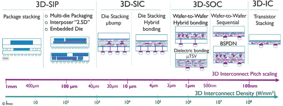
Hybrid bonding combines dielectric and copper surfaces to create direct copper‑to‑copper connections, eliminating solder bumps and enabling interconnect pitches below 10 µm. This yields orders‑of‑magnitude higher interconnect density (up to ~250k–1 M interconnects/mm²) and reduces the vertical distance between dies, lowering latency and power. In semiconductor manufacturing, this technology is now integrated into advanced packaging lines at leading-edge fabs and outsourced semiconductor assembly and test (OSAT) facilities.
Precise surface preparation is critical: the dielectric layer must be ultra‑flat with a root‑mean‑square roughness around 0.1–0.2 nm, and copper pads must be recessed by only a few nanometers. Chemical–mechanical planarization (CMP), plasma activation, and sub‑50‑nm alignment are essential steps. These steps are performed using advanced process tools supplied by companies such as Applied Materials, Lam Research, and Tokyo Electron, and are tightly monitored through inline metrology and defect inspection.
Two main bonding modes exist: wafer-to-wafer (W2W) bonding offers the finest pitch but requires chips of equal size. In contrast, die-to-wafer (D2W) bonding can stack known-good dies of different sizes but demands higher placement accuracy. Engineers in foundries and advanced packaging fabs must choose the mode based on yield models, die size, architecture, and capital cost.
Hybrid bonding improves device performance and reliability: direct Cu–Cu connections reduce parasitic resistance and inductance, enabling higher bandwidth memory (HBM4) with up to 2 TB/s per stack and supporting 12‑ to 16‑layer HBM stacks. The absence of solder eliminates electromigration issues, and the fine pitch improves thermal spreading.
Challenges remain: controlling warpage (<100 µm), managing particles that cause voids, mitigating copper oxidation, ensuring robust metrology, reducing cost, and developing design/IP standards are active research areas. Future developments include polymer‑based low‑temperature bonding, backside power delivery, interlayer cooling, and integration of photonics.
Introduction
As Moore’s law slows and transistor scaling approaches physical limits, advanced packaging has emerged as a primary engine for performance scaling in microelectronics systems. Modern workloads—especially artificial intelligence training and inference, high-performance computing (HPC), and graphics-intensive applications—demand enormous memory bandwidth and ultra-low latency. By stacking chips in three dimensions, engineers can shorten interconnect lengths, increase bandwidth, and integrate heterogeneous functions on a single module. Traditional chip packaging and interconnect methods, such as micro-bumps and through-silicon vias (TSVs), are reaching their practical limits. They constrain interconnect density, increase power consumption, and limit the potential of multi-die systems.
To address these challenges, the industry is turning to advanced 3D integration and next-generation interconnect technologies. Among these, hybrid bonding has emerged as a leading approach. Hybrid bonding is a key enabler of these 3D architectures because it forms direct, adhesive‑free contacts between the metal pads and the surrounding dielectric.
For digital design engineers, hardware architects, and electronics students, understanding hybrid bonding is essential for leveraging new platforms such as 3D high‑bandwidth memory (HBM), chiplet‑based system‑on‑integrated‑chips (SoIC), and heterogeneous integration of logic, memory, and sensors. This article provides a technical overview of hybrid bonding, covering the underlying theory, materials, process flows, benefits, challenges, and implementation considerations.
The Scaling Problem: Why Traditional Packaging Hit a Wall
Traditional 2D integrated circuits rely on wire bonding or solder bumps to connect different dies. Wire bonds introduce long signal paths and high parasitic inductance, while micro‑bumps (µ‑bumps) have pitch limits around 20–50 µm and height of 10–25 µm. As system‑in‑package designs increase in complexity, the number of I/Os per die scales, making the area consumed by solder balls unsustainable. Hybrid bonding addresses these problems by directly joining the metallization and dielectric surfaces, producing extremely short interconnects with minimal parasitic effects. Because the process is performed at near‑room temperatures and uses van der Waals forces followed by thermal annealing, it avoids the high‑temperature reflow required for solder and reduces thermal stress.
The result is an interconnect technology that offers interconnect densities 15 times higher than previous generations, enabling vertical integration of logic and memory, sensors, RF, and photonics. For example, Sony’s CMOS image sensors use hybrid bonding to connect pixel arrays to logic circuits at 6 µm pitch. More recently, TSMC and SK Hynix have deployed HBM4 memory stacks with 12 and 16 layers, delivering up to 2 TB/s bandwidth by bonding thinned DRAM dies directly to logic dies.
Fundamentals of Hybrid Bonding
What Is Hybrid Bonding?
Hybrid bonding is an advanced semiconductor interconnect technology that simultaneously establishes mechanical and electrical connections between two dies or wafers without the need for traditional solder micro-bumps. It achieves this by combining oxide-to-oxide bonding and copper-to-copper bonding on the same interface.
Oxide-to-oxide bonding forms a strong mechanical interface by bringing dielectric surfaces into close contact, creating covalent-like bonds that hold the dies together.
Copper-to-copper bonding enables direct electrical conduction between corresponding pads, providing a low-resistance, high-bandwidth path for signals and power.
By integrating these two bonding mechanisms simultaneously, hybrid bonding eliminates the need for solder bumps, allowing for finer interconnect pitches, reduced vertical distance between dies, and improved reliability. This dual bonding approach is the key enabler for next-generation 3D integration, high-bandwidth memory, and heterogeneous chiplet architectures.
Bonding Physics
The physics behind hybrid bonding is rooted in surface chemistry, precision planarization, and atomic diffusion. Several critical steps ensure a reliable bond:
Surface Activation – Before bonding, both the copper and dielectric surfaces are treated with plasma or chemical activation. This step removes native oxides, increases surface energy, and prepares the surfaces for strong adhesion.
CMP Flatness Requirements – Chemical–mechanical planarization (CMP) is used to achieve ultra-flat surfaces. The root-mean-square (RMS) roughness of the dielectric is typically targeted below ~0.2–0.3 nm, while copper pads are recessed only a few nanometers to ensure intimate contact without damaging the interconnect.
Van der Waals Forces and Copper Diffusion – Once aligned and pressed together, the surfaces adhere through van der Waals forces, enabling the copper atoms to diffuse across the interface during annealing. This atomic diffusion establishes a robust electrical connection, effectively forming a single continuous copper path.
Annealing Steps – Thermal treatment further strengthens both the copper and dielectric bonds. Annealing promotes atomic interdiffusion, relieves stress, and ensures mechanical stability, completing the hybrid bond.
Together, these physics-driven steps produce an interface that is mechanically robust, electrically conductive, and capable of supporting ultra-fine interconnect densities. Extensive electrical and materials characterization—including contact resistance measurement, void inspection, and thermal cycling—is required to ensure long-term bond integrity in high-volume manufacturing.
Recommended Reading: High Bandwidth Memory: Concepts, Architecture, and Applications
Interconnect Pitch & Density
One of the defining advantages of hybrid bonding is its extremely fine interconnect pitch, which can reach less than 10 µm in leading implementations. By eliminating solder bumps and reducing vertical spacing, hybrid bonding allows orders-of-magnitude higher interconnect densities compared to traditional micro-bump stacking. Typical densities in advanced research demonstrations range from ~250,000 to 1,000,000 interconnects per square millimeter, depending on pitch and process node.
The reduced vertical distance between dies also shortens interconnect lengths, minimizing parasitic resistance and inductance. This vertical interconnect shortening not only improves signal integrity and power efficiency but also enables tighter stacking of multiple dies, supporting architectures such as 12-high HBM stacks and future designs that may go beyond 16 layers.
By combining ultra-fine pitch with high interconnect density, hybrid bonding establishes the foundation for high-bandwidth, low-latency, and power-efficient 3D semiconductor systems.
Bonding Modes: Wafer‑to‑Wafer vs Die‑to‑Wafer vs Die‑to‑Die
Hybrid bonding can be performed in three configurations:
Wafer‑to‑Wafer (W2W): Two fully processed wafers are bonded face‑to‑face. Because all dies are bonded collectively, W2W offers high throughput, uniformity, and the finest pitch. However, it requires the dies on both wafers to be the same size and yield; a single defective die can reduce the yield of the entire wafer. W2W hybrid bonding currently achieves commercial pitches down to 6 µm, and research has demonstrated ~400 nm pitch using hexagonal pad patterns and SiCN or SiO₂-based dielectric.
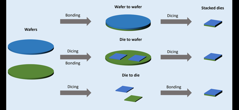
Die‑to‑Wafer (D2W): Known‑good dies are individually placed onto a target wafer. D2W is more flexible, allowing different die sizes and yields, but the placement accuracy must be extremely high because the pitch is approaching a few micrometers in commercial production, not 1 µm yet. Intel notes that as hybrid bonding pitch scales toward 1 µm and below in research, entire chiplet areas must achieve tens‑of‑nanometer placement accuracy [1]. Warpage and die shape distortion become major challenges, requiring new alignment strategies and in‑situ metrology.
Die‑to‑Die (D2D): Individual dies are bonded together outside of a wafer context. D2D is used for small‑volume products or prototypes and may be combined with sequential stacking. Its equipment requirements are similar to D2W, but throughput is lower.
The choice between W2W and D2W depends on factors such as die size, yield, manufacturing infrastructure, and whether the design requires stacking of heterogeneous chiplets. For example, high‑volume CMOS image sensors typically use W2W because the sensor die and logic die are identical in size and yield, whereas heterogeneous chiplet systems like AMD’s MI300A accelerator require D2W assembly to combine different dies.
The table below shows the comparison of different bonding modes.
| Definition | Bonding two fully processed wafers face-to-face | Placing individual known‑good dies onto a target wafer | Bonding individual dies outside a wafer context |
| Throughput | Very high (entire wafer bonded at once) | Moderate (individual die placement) | Low (manual or small‑scale bonding) |
| Alignment Accuracy | ~100 nm overlay | Tens of nanometers for research; commercial slightly larger | Tens of nanometers, similar to D2W |
| Pitch Capability | Commercial down to ~6 µm; research ~400 nm | Approaching a few µm commercially; 1 µm research-level | Similar to D2W; small-area research prototypes |
| Die Size Flexibility | Limited; wafers must have identical die size and layout | High: allows heterogeneous die sizes and known-good dies | High; individual dies can differ |
| Yield Sensitivity | Very sensitive; single defective die reduces wafer yield | Lower sensitivity; only the defective die is wasted | Moderate; small-volume risk is manageable |
| Typical Use Cases | High-volume, uniform dies (e.g., CMOS image sensors) | Heterogeneous chiplet stacking (e.g., AMD MI300A) | Prototypes, low-volume, experimental designs |
| Equipment Complexity | Standard W2W bonding tools | High; requires precise pick-and-place bonding tools | Similar to D2W but lower throughput |
| Advantages | Finest pitch, uniformity, high throughput | Flexibility, known-good-die stacking, heterogeneous integration | Prototype-friendly, flexible design, sequential stacking |
| Limitations | Inflexible die size, yield impact | Placement accuracy is critical, higher equipment cost | Low throughput, less suitable for mass production |
Process Flow and Manufacturing Steps
Hybrid bonding involves multiple process steps that must be tightly controlled to ensure high yield and reliability:
Copper Pad Formation and Planarization
Each wafer starts with the fabrication of copper damascene pads. Copper is deposited in trenches etched into the dielectric and then planarized using chemical–mechanical planarization (CMP). CMP must produce an ultra‑flat surface with minimal dishing and erosion; over‑polishing or under‑polishing can lead to voids or misalignment. Advanced CMP processes combined with surface metrology help achieve the required flatness (Rq < 0.2 nm).
Surface Cleaning and Activation
After planarization, the surfaces undergo pre‑bond cleaning to remove organic contaminants and native oxides. Acidic solutions such as diluted hydrochloric acid or citric acid can reduce copper oxide and allow bonding at temperatures as low as 250 °C. The wafers are then transferred to a vacuum or inert environment and exposed to plasma or ion beam activation, which increases surface energy and enhances van der Waals adhesion. Surface activation also removes adsorbed water and passivates dangling bonds.
Alignment and Initial Contact
In the bonding tool, the wafers or dies are aligned using optical alignment marks. For W2W bonding, the overlay accuracy is typically better than 100 nm; for D2W and D2D, placement accuracy must be tens of nanometers. Alignment tools use through‑silicon illumination and pattern recognition to align the wafers. Once aligned, the surfaces are brought into contact at room temperature, and van der Waals forces cause the dielectric layers to adhere, creating a “pre‑bond.” A narrow gap remains between the copper pads to prevent oxidation.
Annealing
The bonded stack is annealed to achieve strong dielectric bonding and copper diffusion. According to process guidelines, an initial low‑temperature anneal (around 200 °C) increases the dielectric bonding energy and ensures hermetic sealing; a subsequent higher‑temperature anneal (250–400 °C) promotes copper expansion and diffusion. IMEC’s experiments with hexagonal pad grids show that a 350 °C anneal yields low contact resistance and reliable bonds at pitches as small as 400 nm [2]. For polymer hybrid bonding, lower annealing temperatures (<250 °C) combined with pressure control can reduce warpage and particle sensitivity.
Post‑bond processing and thinning
After annealing, the bonded wafers may undergo wafer thinning to remove the handle wafer and reduce stack thickness. Backgrinding followed by stress relief and chemical polishing is used to thin the wafers to tens of micrometers. In some processes, the top wafer is thinned before bonding (for example, in HBM stacks). Further steps may include through‑silicon via (TSV) formation, redistribution layer (RDL) build‑up, and bumping for external connections.
Benefits and Performance Advantages
Density and Pitch Scaling
Hybrid bonding achieves bump pitches below 10 µm and is scaling towards a few micrometers in commercial production, with ~1 µm demonstrated in research, compared with 20–50 µm for µ‑bumps and >90 µm for Cu pillar bumps. The interconnect height effectively becomes very small (not literally zero) because the copper pads reside within the dielectric; this short vertical path reduces signal delay and power consumption. IMEC demonstrated 400 nm pitch with 150 nm overlay accuracy using a hexagonal pad pattern, indicating that monolithic-like connectivity is possible without full monolithic integration.
Electrical Performance
Direct Cu–Cu interconnects have lower resistance and inductance than micro‑bump connections, improving signal integrity and bandwidth. In 2026, TSMC’s 6 µm SoIC hybrid bonding demonstrated up to ~15× increase in interconnect density in test structures, and reduced the vertical distance between logic and memory to a few microns [3]. This “bumpless” architecture can reduce latency significantly (~tens of percent, depending on design) and improve energy efficiency. The high interconnect density allows memory interfaces with thousands of wires, enabling HBM4 stacks to achieve multi-terabyte-per-second bandwidth per stack (~2 TB/s roadmap target, research-level).
Power and Thermal Advantages
The shorter interconnects reduce parasitic capacitance and enable lower operating voltages, decreasing overall power consumption. Hybrid bonded stacks also allow denser heat spreading because the copper pads act as micro‑heat sinks. Combined with a thin die, this reduces thermal resistance and improves cooling. Novel integration schemes, such as direct liquid cooling through micro-channels, are being explored for 3D stacks dissipating >300 W/cm². Hybrid bonding also eliminates solder, removing solder-related failure mechanisms such as electromigration and tin whiskers, which improves reliability.
Reliability and Yield
Without solder, hybrid bonds exhibit superior mechanical strength and fatigue endurance. The oxide layer helps absorb thermal stress and prevents copper extrusion. IMEC reports that hybrid bonded stacks maintain low contact resistance over thermal cycling and stress tests, demonstrating high-quality bond interfaces validated through electrical and materials characterization. The direct interface also reduces contact voids and humidity penetration compared with micro‑bump technology, leading to improved long-term reliability.
Challenges and Limitations
Despite its advantages, hybrid bonding faces several engineering challenges that must be addressed to achieve high-volume manufacturing and reliability.
Surface Quality and Contamination
Hybrid bonding requires an extremely smooth surface with minimal defectivity. Particles left from wafer dicing, CMP slurry, adhesives, and backgrinding can cause voids at the bond interface. Dielectric roughness and copper pad pitting can also degrade bond integrity. To mitigate this, stringent cleaning protocols, protective coatings during die handling, and plasma dicing are used. Large-area surface metrology and inline statistical process control help detect excursions.
Warpage and Mechanical Stress
Thinning wafers to tens of micrometers increases warpage, especially when stacking multiple dies with different materials. Warpage greater than ~100–150 µm (depending on wafer size and tool capability) can cause misalignment during bonding; thus, the warpage must typically be controlled below ~100 µm for advanced nodes. Stress management techniques include using symmetric die stacks, adding carrier wafers during processing, and designing redistribution layers to minimize thermal expansion mismatch.
Alignment Accuracy and Metrology
As pitches scale to a few micrometers in production and toward ~1 µm in research, the required placement accuracy reaches tens of nanometers. This pushes the limits of current bonder equipment and requires improved alignment mark strategies, intra-die distortion compensation, and in-situ metrology. Tools must account for die shape, stress, and temperature gradients. For wafer-to-wafer bonding, overlay errors must be well below the interconnect pitch (often <100 nm in production; <50 nm in advanced research demonstrations) to ensure electrical continuity.
Copper Oxidation and Bulging
Copper readily forms an oxide layer when exposed to air, which inhibits diffusion bonding. Surface activation bonding (SAB) and plasma cleaning can remove oxides and allow low-temperature or near-room-temperature Cu–Cu bonding (often followed by annealing). However, as pitch scales down, the copper volume in each pad decreases and the barrier metal occupies a larger fraction of the pad, raising questions about whether there will be enough copper to achieve full diffusion. Bulging due to copper expansion during annealing must also be controlled to avoid shorting adjacent pads. Alternative metals such as ruthenium or barrier-engineered structures are being investigated.
Cost and Cycle Time
Hybrid bond fabrication involves multiple expensive steps—CMP, cleaning, plasma activation, alignment, bonding, and annealing—that increase cycle time and cost. Innovation toward simplified processes, such as polymer-assisted hybrid bonding that operates at lower pressure and temperature, could reduce costs and improve adoption. Standardized design rules, interface IP, and automated verification tools are also needed for chiplet integration across different vendors.
Thermal Management
Stacking multiple active dies increases thermal density, leading to hotspots. Backside power delivery networks (BSPDN) and interlayer cooling micro-channels are emerging solutions. Thermal simulations by IBM and IMEC show that die order (logic-on-top vs memory-on-top) and cooling strategy significantly affect temperature rise. Designers must include thermal co-design and consider microfluidic cooling or high-thermal-conductivity layers when adopting hybrid bonding in high-power systems.
Current Applications
Hybrid bonding is rapidly transitioning from research to commercial products across several domains:
CMOS Image Sensors
Sony pioneered large-scale commercial hybrid bonding adoption in stacked CMOS image sensors, bonding a pixel array to a logic die at ~6 µm pitch to improve signal integrity and noise performance [4].
High-Bandwidth Memory (HBM)
HBM3 and next-generation HBM (HBM3E/HBM4 roadmap) stacks use hybrid bonding to connect DRAM dies directly to the logic base, eliminating micro-bumps and enabling 12-high stacks in production and 16-high configurations in advanced designs, with roadmap bandwidths approaching or exceeding ~2 TB/s per stack.
Adeia’s DBI Ultra platform (Direct Bond Interconnect) provides room-temperature oxide and metal bonding technology and has been licensed by Kioxia and Western Digital for certain 3D NAND and memory applications [5].
3D Processors and AI Accelerators
AMD’s 3D V-Cache and MI300A architectures stack cache or compute dies on logic dies using hybrid bonding, achieving large on-package SRAM and improved latency. Public details on NVIDIA’s Rubin architecture and its exact bonding method remain limited; future AI accelerators are expected to leverage advanced packaging such as hybrid bonding and SoIC-class technologies.
Heterogeneous Chiplets
Hybrid bonding allows integration of different functions—logic, memory, RF, power management, photonics—on a single package. For example, TSMC’s CoWoS platforms (including CoWoS-L) integrate multiple SoCs and HBM stacks in a single module, while chiplet-as-coolant concepts explore stacking thermal management chiplets with through-silicon micro-channels.
Sensors and Optoelectronics
3D stacked sensors for LiDAR, time-of-flight, and other imaging applications benefit from the small pitch and high interconnect density of hybrid bonding, enabling integration of sensor pixels with analog/digital circuitry. Glass waveguides and co-packaged optics are under development for high-speed data links.
Future Outlook and Emerging Trends
Pitch scaling beyond 1 µm
Research at Intel, IMEC, and other organizations aims to push the hybrid bonding pitch below 1 µm. Achieving such pitches will demand placement accuracies of <10 nm, new metrology method,s and possibly new pad materials. Innovations such as barrier‑less copper alloys, ruthenium interconnects, or novel dielectric liners may enable diffusion at lower temperatures.
Polymer and organic dielectrics
Hybrid bonding uses inorganic dielectrics like SiO₂, but polymer dielectrics are emerging to reduce thermal budget and warpage. Polymers offer low modulus and adjustable CTE, which can match the thermal expansion of different dies. Toray demonstrated polymer hybrid bonding with warpage as low as 13 µm for a 13 × 6 mm chip. Organic dielectrics also enable bonding at temperatures below 250 °C, reducing damage to temperature‑sensitive devices.
Backside power delivery and 3D integration
Backside power delivery networks (BSPDN) separate power planes from signal wires, reducing IR drop and allowing more routing layers on the front side. When combined with hybrid bonding, BSPDN enables the stacking of logic and memory dies without large copper bumps. However, BSPDN introduces new thermal challenges; careful modeling and microfluidic cooling are required. These developments point toward monolithic 3D integration where logic and memory are integrated as one continuous stack.
Glass substrates and system‑on‑wafer packaging
By the late 2020s, the industry is expected to transition to glass substrates for packaging. Glass offers superior flatness and thermal stability, enabling 10× higher routing density and large system‑on‑wafer designs that integrate dozens of chiplets. Hybrid bonding will likely be the interconnect of choice in these packages, connecting chiplets to the glass carrier and to each other. Integration with co‑packaged optics could deliver energy‑efficient data links over tens of centimeters.
Environmental and economic considerations
While hybrid bonding improves performance, the environmental impact of 3D stacked chips is significant: manufacturing complexity may lead to a 16‑fold increase in CO₂‑equivalent emissions from GPU production by 2030. Data centers will require enhanced cooling, such as liquid or interlayer cooling. Economically, advanced packaging is becoming the profit center of the semiconductor supply chain; TSMC’s advanced packaging revenue is projected to reach $18 billion in 2026 [3]. Engineers should consider sustainability and cost when adopting hybrid bonding.
Conclusion
Hybrid bonding is transforming the landscape of digital design and hardware engineering. By enabling sub‑10 µm pitches and direct copper‑to‑copper connections, it offers unprecedented interconnect density, lower power consumption, and improved thermal performance. These benefits are critical for scaling AI accelerators, memory stacks and heterogenous systems beyond the limits of conventional planar integration. However, achieving reliable hybrid bonds requires careful attention to surface preparation, alignment, warpage control and thermal design. Future developments—including polymer dielectrics, backside power networks, glass substrates and optical integration—will further push the boundaries of 3D integration.
As the semiconductor industry enters a “Packaging‑First” era, engineers must become proficient in hybrid bonding to design the next generation of high‑performance, energy‑efficient systems.
Frequently Asked Questions (FAQ)
Q1: What is the difference between hybrid bonding and micro‑bumping?
Micro‑bumping uses solder balls (µ‑bumps) to connect dies, with typical pitches of 20–50 µm. Hybrid bonding eliminates solder entirely; copper pads recessed within a dielectric are directly bonded, achieving pitches below 10 µm and potentially down to 1 µm. The result is much higher interconnect density, lower resistance and no solder‑related reliability issues.
Q2: Why is surface roughness so important in hybrid bonding?
Because the dielectric–dielectric bond is formed via van der Waals forces, any particles or roughness can prevent intimate contact and create voids. Metrology guidelines recommend dielectric roughness around 0.1–0.2 nm and copper recess depths of 1–5 nm. Achieving these tolerances requires precise CMP and cleaning. Large‑area profilometry ensures the wafer remains flat across millimeter‑scale distances.
Q3: How do I choose between wafer‑to‑wafer and die‑to‑wafer hybrid bonding?
W2W bonding offers the smallest pitch and highest throughput but requires identical die sizes and yields. D2W allows stacking known‑good dies of different sizes but demands extremely accurate placement (tens of nanometers) and careful warpage control. For heterogeneous chiplet designs or when yield is a concern, D2W is preferred. For homogenous die stacks like image sensors or memory, W2W may be more efficient.
Q4: What are the main reliability challenges for hybrid‑bonded stacks?
Key challenges include warpage, particle contamination, copper oxidation and thermal management. Warpage must be kept below 100 µm and particles from dicing or backgrinding can cause voids. Copper surfaces must be protected from oxidation, often via plasma activation or surface‑activated bonding. Stacked dies generate more heat, requiring careful thermal design and possibly interlayer cooling.
Q5: Can hybrid bonding be applied at low temperatures?
Standard hybrid bonding uses annealing temperatures of 250–400 °C to facilitate Cu diffusion. However, research into low‑temperature polymer hybrid bonding shows that bonding below 250 °C with organic dielectrics can achieve high yield and reduce warpage. Surface‑activated bonding techniques can also produce Cu–Cu bonds at near room temperature.
Q6: How does hybrid bonding affect system design?
Hybrid bonding enables chiplets to be arranged vertically, affecting architectural choices. Designers can place memory directly on top of compute logic to shorten data paths, or stack analog and digital sensors. However, the vertical integration complicates power delivery and thermal management. Design tools must support multi‑die co‑optimization, and standards for hybrid bond IP and design rules are evolving.
Q7: What future technologies could enhance hybrid bonding?
Emerging trends include backside power delivery networks (moving power lines to the wafer backside), integration of microfluidic cooling channels, adoption of glass substrates for system‑on‑wafer packaging, and co‑packaged optics for high‑bandwidth communication. Ongoing research aims to reduce bond pitch below 1 µm and explore barrier‑less metals or novel dielectrics to further lower the temperature and increase reliability.
References
[1] Intel Corporation, “Foveros Direct 3D: Enabling Sub-10 µm Hybrid Bonding for Advanced Chiplet Integration,” 2023. [Online]. Available: Link
[2] IMEC, “Advanced Hybrid Bonding for Sub-Micron Interconnect Scaling,” 2022–2024. [Online]. Available: Link
[3] TSMC, “System on Integrated Chips (SoIC™) Technology,” TSMC Technology Symposium Materials. [Online]. Available: Link
[4] Sony Semiconductor Solutions Corporation, “Stacked CMOS Image Sensor Technology,” Technical Overview. [Online]. Available: Link
[5] Adeia Inc., “DBI® Ultra Hybrid Bonding Platform,” 2023–2024. [Online]. Available: Link
in this article
1. Key Takeaways2. Introduction3. The Scaling Problem: Why Traditional Packaging Hit a Wall4. Fundamentals of Hybrid Bonding 5. Bonding Modes: Wafer‑to‑Wafer vs Die‑to‑Wafer vs Die‑to‑Die6. Process Flow and Manufacturing Steps7. Benefits and Performance Advantages8. Future Outlook and Emerging Trends9. Conclusion10. Frequently Asked Questions (FAQ)