Featured
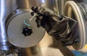
Solder flux has a large impact on final product quality. This article reviews how to use flux during soldering and how to decide on the right technology options for your project.
Solder flux has a large impact on final product quality. This article reviews how to use flux during soldering and how to decide on the right technology options for your project.
PCB Trace Width Calculator
Glossary of Semiconductors Terms
Solder flux has a large impact on final product quality. This article reviews how to use flux during soldering and how to decide on the right technology options for your project.
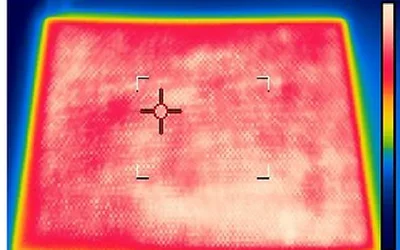
Sometimes manufacturers would like to install heating in objects that are difficult to heat. The armrest of your car. Your sporty winter coat. Bags for food delivery. Sleeping bags. etc This has been difficult to achieve until now. Read more about printed heater technology
Proven benchmarks provide a structured method for comparing ML/DL products and services.
Semiconductors are the building blocks of modern electronics, powering everything from smartphones to satellites. This in-depth guide provides a comprehensive understanding of semiconductors' engineering principles and applications, delving into their fundamental concepts, materials, devices, manufacturing processes, and their impact on today's technology landscape.
13 minutes read.
20 minutes read.
16 minutes read.
20 minutes read.
20 minutes read.
13 minutes read.


Semiconductors
Nordic Semiconductor is a fabless semiconductor company specializing in wireless technology that powers the IoT.
181 Posts
A guide covering the full radio-frequency design workflow, starting from setting specifications and choosing topologies to matching, simulation, layout, and verification, to help antenna engineers.
This article presents a detailed technical exploration of SiC MOSFET devices, covering material physics, device structure, switching behavior, and practical design considerations for high-efficiency power electronics systems.
This article is a comprehensive technical guide to relay wiring diagrams, covering 4-pin and 5-pin configurations, working principles, safety practices, standards, and advanced relay applications in modern systems.
Explore how frequency shapes EMC behavior from RF emissions to ultra-low-frequency drift, with mitigation strategies for robust, compliant electronic system design.
How Essentra Components Supports Engineering from Concept to Production
Makera gives live demonstrations of the Z1 during the 2026 Hackaday Europe event. The Z1 is a compact CNC manufacturing platform.
A crystal oscillator is an electronic circuit that uses a quartz crystal to produce a precise and stable frequency reference. This article covers crystal operation, equivalent circuit models, resonance, load capacitance, oscillator topologies, stability, aging, and design practices.
June 25, 2026 at 08:00 PM Central European Summer Time
Solder flux has a large impact on final product quality. This article reviews how to use flux during soldering and how to decide on the right technology options for your project.

4 minutes read
Sometimes manufacturers would like to install heating in objects that are difficult to heat. The armrest of your car. Your sporty winter coat. Bags for food delivery. Sleeping bags. etc This has been difficult to achieve until now. Read more about printed heater technology

2 minutes read
Proven benchmarks provide a structured method for comparing ML/DL products and services.
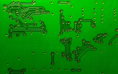
Printed Circuit Board Vertical Interconnect Access (PCB VIAs) are small plated holes that create electrical connections between different circuit board layers. This article delves into the various types, functions, and best practices of PCB VIAs to help you optimize your PCB design.
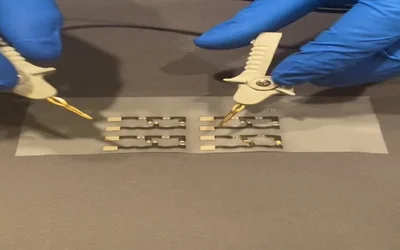
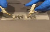
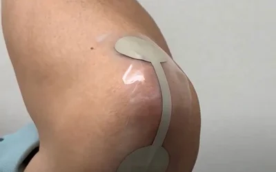
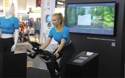
Wearable electronic textiles are a demanding environment for reliable interconnects – the ability to function with movement and survive multiple cleanings and reuse. Good adhesion is particularly challenging in these wearable and conformable electronics applications. While solders provide the most conductive electrical connection, they are rigid and require not only the addition of an underfill adhesive but usually a post bond encapsulation. This Anisotropic Conductive Epoxy, provides reliable interconnections between electronic components and circuitry on textiles with excellent structural bonding, without encapsulation, even under repeated stretching and washings. This technology has been shown as a scalable assembly process for e-Textile manufacturing in an SMT line.
5 minutes read
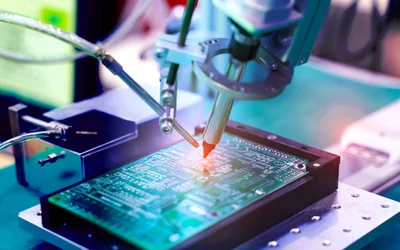
Your new PCBA project design needs to pass production validation testing (PVT) to prove it's ready for production. The planning you did for cost, quality assurance, quality control, and scalability now positions your project for success.
3 minutes read
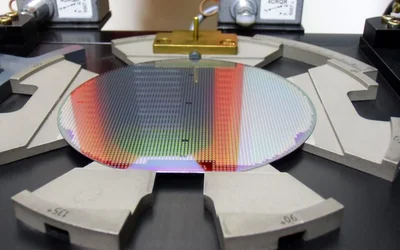
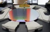
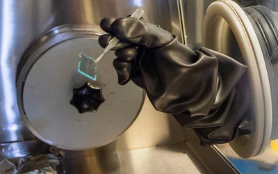
Wafer thinning is a part of the semiconductor manufacturing process. It is essentially grinding off the backside of the wafers to control their thickness and is useful for the production of ultra-thin wafers. These flattened wafers are used to effect stacked and high-density packaging in compact or microelectronic devices. This article discusses the meaning of wafer thinning, along with its various techniques and significance.
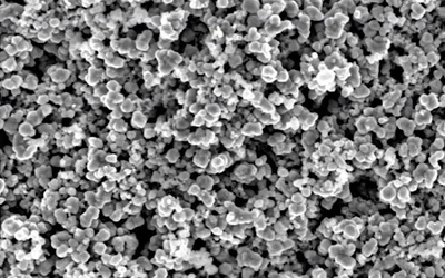
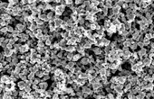
Cost of production has been a major barrier despite the fact that Cu raw material prices are far lower than Ag. This is because this large raw material cost difference does not often get translated into equally large nanoparticle dispersion or ink costs. Can this be overcome?
In general, silicone based conductive pastes are rare and the versions with AgCl fillers- needed for many medical wearable applications- are even rarer!
Warp knitting is an excellent candidate. It combines weaving and weft knitting, allowing the warp knitted fabrics to have the stability of woven fabrics and the elasticity of knitted ones.
Conformal EMI shielding is a megatrend on its way to become ubiquitous in electronics. The incumbent process is based on sputtering a tri-layer structure consisting of SUS on the EMC of the package. In these slides, you can see performance analysis and detailed cost analysis/projections.
2 minutes read
The progress of screen printing towards fine line printing has been incredible going from 100 µm features before 2010 to 70 µm to 2015 to 40 µm in 2018 and now pushing - in development- towards 20 µm and less. In parallel, the wet thickness of the printed line have gone down from 12um or so in 2018 to now just 4um.
As microLEDs inevitably shrink in size, the micro-bumping requirements for the microLED dies becomes more challenging. Direct wafer-based printing based on gravure offset techniques offers a promising solution in this regard. Indeed, this is another field where printed electronics can play a role.
The three themes are closely linked since QDs can be digitally printed as color conversation materials atop blue microLEDs to enable wide color gamut RGB uLED displays without requiring a separate transfer step for each color.. This is an important technology as it simplifies the manufacturing step for microLED and thus removing a major hinderence.
The new approach moves energy efficiently and could reduce energy losses converting light into electricity.

3 minutes read