Understanding Logic Gate Symbols: Comprehensive Guide for Engineers
This article provides a detailed examination of logic gate symbols, truth tables, and transistor level implementations, with practical insights for digital design and hardware professionals.

30 Jan, 2026. 15 minutes read
Key Takeaways
Logic gates are the fundamental building blocks of digital circuits; understanding their symbols and truth tables is essential for engineers.
Two standardized symbol sets exist - distinctive‑shape and rectangular‑shape - as defined by IEEE/ANSI and IEC standards.
Universal gates such as NAND and NOR can implement any logic function, illustrating functional completeness.
Transistor‑level implementations differ by logic family (e.g., CMOS, TTL, ECL); CMOS offers low power consumption while TTL provides high speed.
Modern hardware designs pack billions of transistors into integrated circuits; Apple’s M3 Ultra SoC (2025) contains ~184 billion transistors.
Introduction
Today, the digital systems, from tiny IoT devices to powerful data‑center processors, process information using binary logic. The logic gates implement Boolean functions that control how bits flow through circuits. The clear understanding of logic gate symbols enables engineers to read schematics accurately, identify functional blocks, and troubleshoot complex designs without ambiguity.
In modern hardware design, logic gate symbols act as a universal language across datasheets, simulation tools, and PCB schematics. Whether working on microcontroller interfaces, programmable logic devices, or discrete digital circuits, engineers rely on these symbols to visualize Boolean operations and signal flow. Misinterpreting logic gate symbols can lead to wrong assumptions, design errors, or inefficient implementations.
This article provides a detailed overview of logic gate symbols, explaining their conventions, variations, and their practical relevance for improving design accuracy, documentation clarity, and collaboration across multidisciplinary engineering teams.
Foundations of Digital Logic and Boolean Algebra
Binary Signals and Boolean Variables
Digital electronics encode information using two discrete voltage levels that represent binary inputs. These levels map directly to Boolean variables, which take the values 0 (false) or 1 (true). In a logic circuit, each input assumes a defined logic state, and the total number of possible input combinations depends on the number of inputs. For a circuit with n inputs, there are 2n possible input states. [1] For example, a two-input circuit has four combinations — (0,0), (0,1), (1,0), and (1,1) — while a three-input circuit has eight. This exponential growth is fundamental to logic design in modern digital systems.
Engineers describe the relationship between input values and output states using truth tables, which provide a complete and unambiguous representation of circuit behavior.
Truth Tables and Logic Expressions
The truth table is a mathematical table used in logic, Boolean algebra, and computer science to list all possible input combinations (usually True/False or binary numbers, 1/0) and the corresponding outputs for a logic function. It maps inputs to an output, providing a complete, organized representation of logical operations like AND, OR, and NOT. [2]
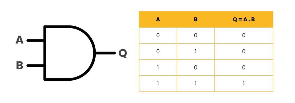
For a two‑input AND gate, the output is true only when both inputs are true, giving the Boolean expression Q (AND) = A ⋅ B. The truth table is:

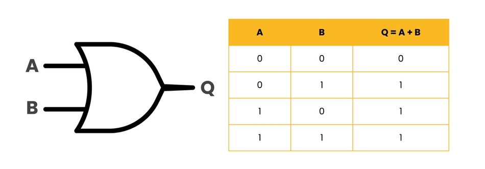
Similarly, a two‑input OR gate produces a true output if either input is true; the Boolean expression states: Q = A + B: The truth table is:
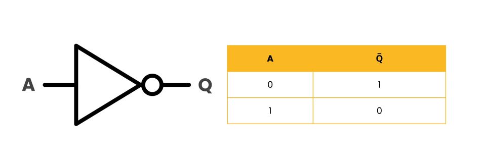
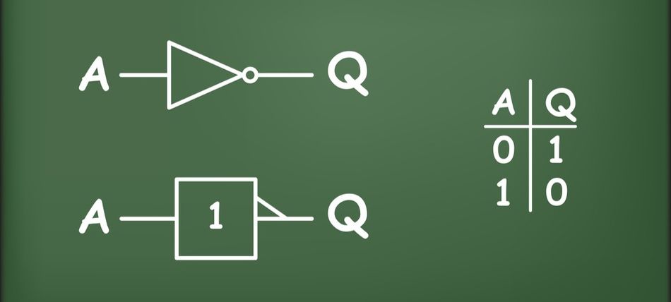
The NOT gate (inverter) outputs the complement of its input; if A is 1, then Q is 0 and vice versa.
These basic logic gates form the building blocks of more complex digital architectures and underpin all higher-level circuit implementations discussed throughout this article.
Recommended Reading: Circuit Symbols: A Comprehensive Guide for Electronics Engineers
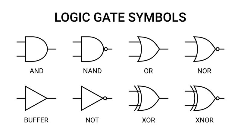
Standard Logic Gate Symbols
Symbol Standards
Logic gate symbols provide a concise visual language for representing logical operations in a schematic or circuit diagram. Two standardized symbol systems are defined in ANSI/IEEE Std 91-1984 and its supplement 91a-1991. [3] The distinctive-shape set uses traditional forms — flat-front symbols for the AND function, curved shapes for OR, and a triangle with a small circle for NOT—originating from MIL-STD-806. The alternative rectangular set represents all gates as rectangles and emphasizes functional labeling rather than shape. This approach is preferred by the IEC standard IEC 60617-12, particularly for complex digital systems and mixed-signal designs. While IEC discourages distinctive shapes, both conventions coexist in practice, and engineers select the style that best suits the application, tooling, or audience.
Inputs, Outputs and Polarity Indicators
Symbols can include bubbles or wedges at inputs or outputs to indicate logic negation. A bubble marks an inversion (logic 0 becomes 1 and vice versa). For example, the NOT (inverter) symbol is a triangle with a bubble on its output. The bubble must be accompanied by a statement specifying the logic convention (whether a high voltage represents 1 or 0). A wedge indicates an active‑low input or output without requiring a uniform convention. Polarity indicators help clarify whether a gate is drawn in positive or negative logic and are essential for understanding De Morgan equivalents.
Basic Gate Symbols and Truth Tables
The following types of logic gates form the building blocks of logic design in computer science, CPUs, and embedded hardware:
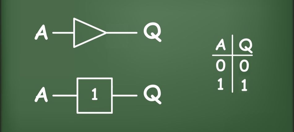
Buffer (Identity Gate)
The buffer outputs exactly what it receives. It has a single input and a single output and is often used to increase drive strength or isolate stages in a logic circuit.
NOT Gate (Inverter)
The NOT gate, or inverter, outputs the complement of its input. The distinctive symbol is a triangle with a bubble at the output.
AND Gate
The AND gate produces a true output only when all binary inputs are true. The distinctive symbol has a flat front.
OR Gate
The OR gate outputs true if any input is true. Its symbol has a curved front.
<grammarly-extension></grammarly-extension><grammarly-extension></grammarly-extension>

NAND Gate
The NAND gate (input NAND gate) outputs the negation of the AND function; it is drawn as an AND symbol with a bubble on the output.
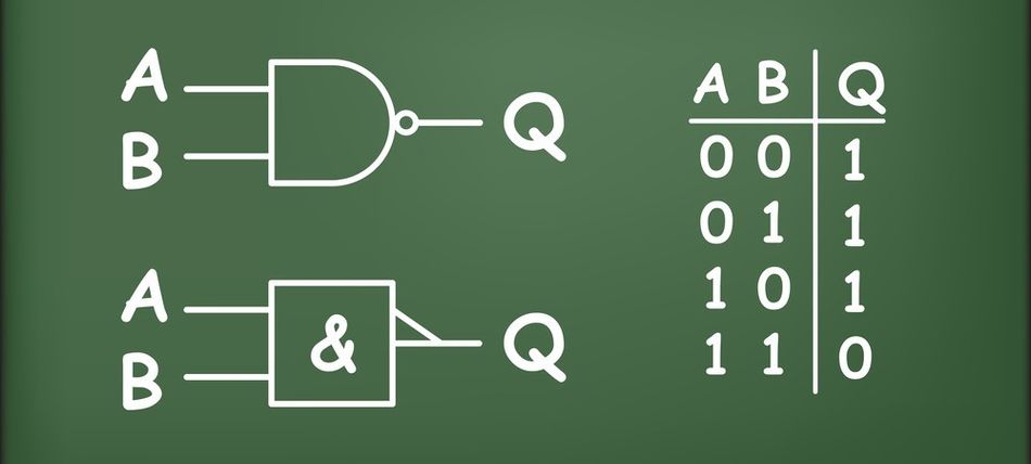
NAND and NOR gates are universal gates because they can implement any Boolean function.
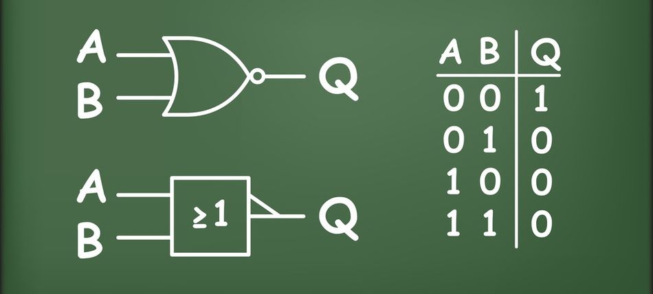
NOR Gate
The NOR gate produces the negation of the OR function. Its symbol is an OR shape with a bubble on the output.
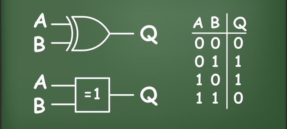
XOR Gate (Exclusive OR)
The ex-or gate (XOR) outputs true if exactly one of the inputs is true. Its distinctive symbol resembles OR but has an additional curved line on the input side.
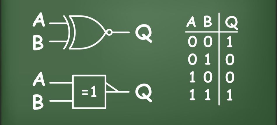
XNOR Gate (Exclusive NOR)
The XNOR gate is the complement of the XOR gate; it outputs true when both inputs are equal.
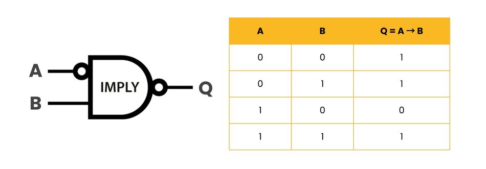
IMPLY and NIMPLY Gates
Less commonly used gates include the implication gate (IMPLY) and the non‑implication gate (NIMPLY). An IMPLY gate outputs false only when A is true, and B is false; the expression yields the truth table:
The NIMPLY gate outputs true only when A is true, and B is false. The expression yields the truth table:
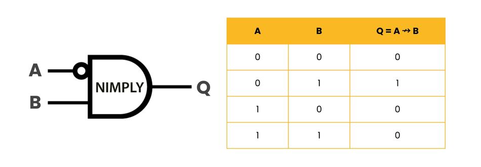
Rarely used in hardware, IMPLY and NIMPLY gates appear in formal Boolean logic and theoretical analysis.
De Morgan Equivalent Symbols and Negative Logic
De Morgan’s laws state that the complement of a conjunction equals the disjunction of the complements, and vice versa. [4] Graphically, this means an AND function with inverted inputs and outputs is equivalent to an OR function, and an OR function with inverted inputs and outputs is equivalent to an AND function. These equivalences lead to alternative symbols - called De Morgan symbols - where the core shape (AND or OR) is swapped, but bubbles denote the proper polarity. Using De Morgan symbols can highlight the primary logical purpose of a gate and clarify active‑low paths. Engineers use them to avoid inadvertently connecting an active‑high output to an active‑low input; matching bubbles cancel, eliminating explicit negations.
Recommended Reading: Half Adder vs Full Adder: Comprehensive Guide for Engineers
Universal Logic Gates and Functional Completeness
Universal Gates
A set of logic gates is functionally complete if any Boolean function can be implemented using only gates from that set. Charles Sanders Peirce and later Henry Sheffer proved that the NOR gate (Peirce’s arrow) and the NAND gate (Sheffer stroke) are each functionally complete. In practice, digital designers frequently choose NAND or NOR gates for entire circuits because they simplify manufacturing and reduce cost. For example, constructing an inverter using only NAND requires tying the inputs together; constructing an AND gate uses two NANDs (one as NAND, one as an inverter).
The table below summarizes how universal gates implement other functions:
| Target Function | NAND Construction | NOR Construction |
| NOT | Connect both inputs of a NAND gate together | Connect both inputs of a NOR gate together |
| AND | NAND followed by NOT | NOR with inverted inputs |
| OR | NAND with inverted inputs | NOR followed by NOT |
| XOR | Combination of several NAND gates | Combination of several NOR gates |
Functional completeness underpins the design of programmable logic arrays and FPGAs, where a limited set of universal gates is used to implement complex functions via configuration.
Recommended Reading: How Does a Transistor Work? Theory & Practical Applications for Engineers?
Transistor‑Level Implementation of Logic Gates
Understanding how gates are built from transistors helps engineers evaluate speed, power consumption and noise margins. The two major logic families - Complementary Metal‑Oxide Semiconductor (CMOS) and Transistor Transistor Logic (TTL) - are widely referenced. This section focuses on CMOS implementations, which dominate modern integrated circuits, and contrasts them with TTL and the high‑speed ECL family.
CMOS Implementation Principles
CMOS gates use complementary pairs of p‑channel (PMOS) and n‑channel (NMOS) MOSFETs.
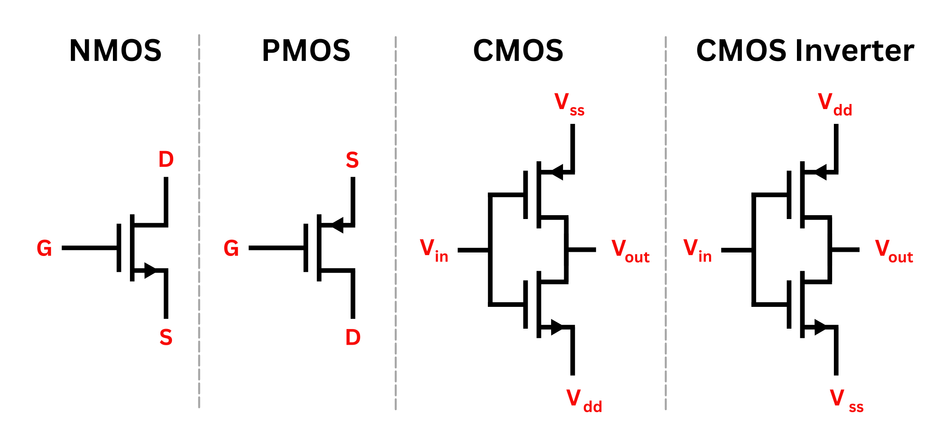
In general, PMOS transistors form the pull‑up network (PUN) connecting the output to the positive supply (+V), whereas NMOS transistors form the pull‑down network (PDN) connecting the output to ground. Inputs drive the gates of both networks simultaneously; only one network conducts at a time, ensuring low static power consumption.
CMOS Inverter (NOT Gate)
A CMOS inverter comprises one PMOS and one NMOS transistor connected in series. The input drives both gates; the output is taken from their drains. When the input is high, the NMOS transistor conducts, and the PMOS is off, pulling the output low. When the input is low, the NMOS is off, and the PMOS conducts, pulling the output high.
CMOS NAND Gate
In a two‑input CMOS NAND gate, PMOS transistors Q1 and Q2 are connected in parallel between +V and the output, while NMOS transistors Q3 and Q4 are connected in series between the output and ground. The output becomes logic 0 only when both NMOS devices conduct simultaneously (inputs A and B are high). For other input combinations, at least one NMOS device is off and at least one PMOS device is on, so the output is pulled high, matching the NAND truth table.
CMOS NOR Gate
A CMOS NOR gate reverses the arrangement: PMOS transistors are connected in series between +V and the output, and NMOS transistors are connected in parallel between the output and ground. The output is pulled high only when both inputs are low; any high input turns on an NMOS transistor, pulling the output low. This satisfies the NOR truth table.
CMOS AND and OR Gates
AND and OR functions are often implemented by combining simpler gates. A CMOS AND gate is a NAND gate followed by a CMOS inverter; the NAND yields - (A·B) and the inverter negates it to produce A·B. A CMOS OR gate is a NOR gate followed by an inverter, producing A + B.
CMOS XOR Gate
Implementing an XOR gate requires more transistors. One approach uses a combination of NOR, AND and OR operations. In a CMOS implementation, four transistors create the NOR function, followed by three more transistors to generate the ANDing and ORing of intermediate signals. Additional transistors invert the result, yielding the XOR truth table. Although more complex, the CMOS XOR gate remains efficient because only one network conducts at any time.
TTL and ECL Logic Families
TTL gates are built from bipolar junction transistors. The inputs of TTL gates are transistor bases, which require current to turn on. Standard TTL devices operate at 5 V and historically ran at speeds up to 25 MHz. The introduction of Schottky-clamped transistor logic reduced storage charge and decreased propagation delay, achieving typical delays around 10 ns. In contrast, the Emitter Coupled Logic (ECL) family used differential pairs for high‑speed switching; ECL gates could achieve propagation delays around 1 ns but consumed significantly more power.
CMOS Advantages
CMOS technology combines p‑channel and n‑channel MOSFETs so that at any moment, one network is off, minimizing static current. Consequently, CMOS gates offer low power dissipation, high noise immunity and scalability to billions of transistors. Engineers value CMOS for battery‑powered devices and high‑density chips because it conserves energy and dissipates little heat. CMOS can operate over a wide range of supply voltages and has become the default for microprocessors, RAM and FPGAs.
TTL vs CMOS Comparison
Selecting a logic family involves trade‑offs in speed, power, noise tolerance and cost. The differences include:
Power Consumption: TTL inputs draw current; typical TTL devices sink up to 1.6 mA per input, which becomes problematic when many inputs are connected. CMOS gates draw almost no DC current, except for leakage and dynamic charging of input capacitances.
Speed: Standard TTL propagation delays are around 33 ns; high‑speed TTL subfamilies reach 6 ns but consume more power. CMOS propagation delay depends on process technology; modern CMOS chips achieve multi‑GHz clock rates and gate delays below 1 ns.
Noise Immunity: CMOS gates have higher noise margins and can tolerate greater input noise, making them suitable for environments with electrical interference. TTL gates have lower noise margins but are less susceptible to electrostatic discharge because bipolar transistors are used.
Fan‑Out: CMOS outputs can drive more inputs thanks to high input impedance and low output impedance, whereas TTL outputs have lower fan‑out capacity.
Ruggedness: TTL devices are generally more rugged; CMOS devices can be damaged by electrostatic discharge because the thin gate oxide of MOSFETs has a low breakdown voltage.
In most modern designs, CMOS supersedes TTL for integrated circuits. TTL chips still appear in legacy equipment and educational laboratories, but rarely in new designs.
Recommended Reading: Concurrent-Mode CMOS Detector IC for Sub-Terahertz Imaging System
Integrated Circuit Families and Manufacturing
Logic Families and Gate Arrays
Several integrated circuit families exist beyond TTL and CMOS. Early families included resistor–transistor logic (RTL) and diode–transistor logic (DTL). TTL replaced DTL for higher speed, and CMOS eventually superseded TTL due to its low power consumption. Modern logic families include low‑power CMOS subfamilies such as HC (High‑speed CMOS) and AC (Advanced CMOS), which optimize speed while retaining low power. The other specialized family, ECL, remains in limited high‑speed applications. Logic gates are available as discrete components or as part of complex integrated circuits.
Integrated Gate ICs
Small‑scale integration (SSI) devices, such as the 7400 series (TTL) and 4000 series (CMOS), package individual gates. A 7400 chip contains four two‑input NAND gates and requires external power pins; integrated circuits like this can be cascaded because outputs can drive multiple inputs. Designers must consider fan‑out limitations - the maximum number of inputs an output can drive - and propagation delay when cascading gates. The ability to cascade gates without concern for internal workings led to the success of standardized IC families. Today, discrete gate ICs are often replaced by programmable logic devices (PLDs) and field programmable gate arrays (FPGAs), which allow configurations of thousands to millions of gates to perform arbitrary logic functions.
Transistor Counts and Moore’s Law
Microprocessors and GPUs integrate millions to billions of logic gates. According to records compiled in 2025, the highest transistor count in a consumer microprocessor is 184 billion transistors in the ARM‑based dual‑die M3 Ultra system‑on‑chip by Apple, fabricated with a 3 nm process. Blackwell B100 GPU by Nvidia contains 208 billion transistors, and specialized deep‑learning processors like Wafer Scale Engine 2 by Cerebras pack 2.6 trillion transistors by using an entire wafer. Flash memory chips push transistor counts further - 232‑layer V‑NAND module by Micron contains 5.3 trillion floating‑gate MOSFETs.
Moore’s law observes that transistor counts double approximately every two years, enabling exponential growth in computational capacity. Process nodes have shrunk from 20 µm in 1968 to 3 nm in 2022 and are projected to reach 2 nm in 2025. As transistors shrink, gate delays decrease, and power efficiency improves, but challenges such as leakage, variability and quantum effects require new materials and device architectures. Engineers must understand how transistor scaling affects gate performance when designing at advanced nodes.
Recommended Reading: RTL Design: Comprehensive Guide to Understanding and Implementing Register-Transfer Level Design
Combinational and Sequential Logic
Combinational Circuits
Combinational logic circuits produce outputs solely based on current inputs. Engineers build complex functions by combining basic gates. The examples include:
Adders: A half‑adder sums two bits using XOR and AND gates; a full adder sums three bits (two inputs and a carry‑in). Cascading full adders creates multi‑bit ripple adders.
Multiplexers: A multiplexer selects one of several inputs to pass to the output based on selection lines; it uses AND, OR and NOT gates.
Decoders: A decoder converts binary inputs into a one‑hot output line; 2‑to‑4 or 3‑to‑8 decoders are common building blocks.
Encoders and priority encoders: The inverse of decoders, they produce binary codes representing the position of a single high input.
Arithmetic logic units (ALUs): Core units in processors, ALUs combine adders, logic gates and shifters to perform arithmetic and logic operations.
Combinational circuits rely on propagation delays of individual gates; designers must calculate the worst‑case delay to ensure proper timing. The fan‑out, hazards and glitches (unintended pulses) are additional considerations. Universal gates can implement any combinational circuit, but gate minimization techniques (Karnaugh maps, Boolean algebra simplification) help reduce complexity.
Sequential Logic and Memory
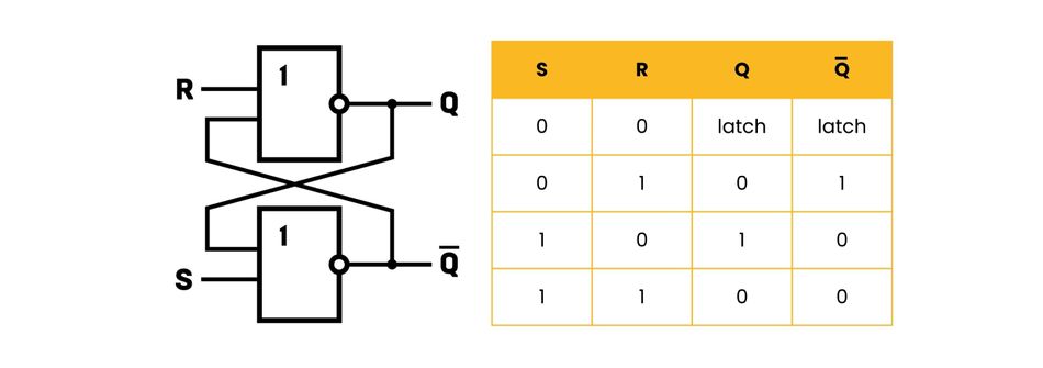
Sequential circuits incorporate storage elements so that outputs depend on both current inputs and previous states. Basic storage elements include latches (level‑sensitive) and flip‑flops (edge‑triggered). A common latch uses cross‑coupled NOR gates; connecting two NOR gates so that each output feeds back into the other yields an SR latch that holds a state until new inputs arrive.
Flip‑flops add clock inputs; the rising or falling edge triggers the state change, enabling synchronization with system clocks. Registers pack multiple flip‑flops to store multi‑bit values. Sequential logic circuits, such as counters, shift registers and finite‑state machines, combine combinational logic with storage elements to implement complex behaviors.
Engineers must consider setup and hold times, clock skew, metastability and synchronous vs asynchronous design when working with sequential logic. High‑density integrated circuits incorporate sophisticated clock trees and timing analysis to ensure reliability.
Recommended Reading: Understanding the SR Latch: Theory, Design, Truth Tables and Practical Implementations
Modern Design Considerations
Hardware Description Languages and Synthesis
As digital circuits grew more complex, manual schematic design gave way to hardware description languages (HDLs) such as Verilog and VHDL. HDLs describe logic behavior textually; automated synthesis tools translate descriptions into gate‑level implementations. The use of HDLs allows engineers to design at a higher level of abstraction and iterate quickly. Even though modern designs often target FPGAs or application‑specific integrated circuits (ASICs), understanding gate symbols and basic logic remains essential for debugging and optimization.
Propagation Delay, Fan‑Out and Noise
In high‑speed systems, the propagation delay of individual gates accumulates through cascaded stages. The input capacitance and output resistance of each gate determine how quickly the output can charge or discharge. TTL propagation delay is typically ~33 ns; low‑power Schottky TTL reduces it to ~10 ns; high‑speed TTL reaches ~6 ns. ECL achieves ~1 ns at the cost of higher power consumption. CMOS propagation delay depends on process technology and transistor sizing; advanced nodes support gate delays below 1 ns and clock frequencies above 4 GHz. Engineers design proper buffering and clock distribution to mitigate skew and maintain timing closure.
The fan‑out limits how many inputs a gate output can drive. Exceeding fan‑out increases load capacitance, slowing transitions and risking logic-level violations. Designers may add buffers or repeaters to increase fan‑out.
The noise immunity, how well a gate withstands voltage noise on inputs, depends on the logic family. CMOS gates have larger noise margins and can operate over a wider voltage range. TTL gates have smaller noise margins but are less susceptible to static discharge. When interfacing different logic families or long interconnects, engineers may need level shifters and proper termination.
Power Consumption and Thermal Management
Power consumption comprises static power (leakage current) and dynamic power (charging and discharging capacitive loads). In CMOS, static power is negligible except at very small nodes, but dynamic power scales with switching frequency, capacitance and supply voltage. Techniques such as clock gating, voltage scaling and power gating reduce power consumption. TTL and ECL draw more static power; thus, they generate more heat even when idle. Thermal considerations include heat‑sink design, airflow and device placement. As transistor counts climb into the hundreds of billions, power management and thermal design become critical.
Emerging Technologies
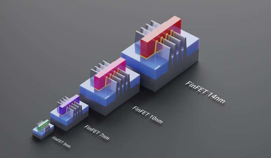
Researchers explore alternatives to CMOS to continue scaling beyond the 2 nm node. FinFETs, gate‑all‑around FETs, tunneling FETs and 2D materials such as graphene and molybdenum disulfide promise improved electrostatics and lower leakage. Meanwhile, spintronic, optical and quantum logic gates offer potential leaps in speed or power efficiency. Engineers must stay informed about these technologies as they transition from research to production.
Recommended Reading: MOSFET Symbol: Theory, Practical Usage and Future Trends
Conclusion
Logic gate symbols and truth tables form the foundational language of digital design, enabling engineers to represent, analyze, and implement Boolean functions within modern digital systems. Whether shown using distinctive or rectangular conventions, these symbols allow clear interpretation of schematics and accurate construction of combinational and sequential circuits. Universal gates illustrate how a small set of building blocks can realize any logic function, while CMOS technology dominates implementation due to its power efficiency and scalability. Although TTL and other families persist in specialized applications, the core concepts of AND, OR, NOT, NAND, NOR, and XOR remain unchanged.
Today, as design shifts toward hardware description languages and reconfigurable platforms, a strong understanding of logic gate symbols continues to support informed decisions in performance, reliability, and power optimization.
Frequently Asked Questions (FAQs)
Q1: Why are there two sets of logic gate symbols?
A: The ANSI/IEEE standard defines distinctive‑shape symbols based on traditional schematics, while the IEC standard prefers rectangular shapes for consistency. Both sets coexist to accommodate different drawing conventions.
Q2: What makes NAND and NOR gates “universal”?
A: A gate is universal if any Boolean function can be built solely from that gate. NAND and NOR gates are universal because you can construct NOT, AND, OR and more complex functions by appropriately wiring their inputs and outputs.
Q3: How does a CMOS NAND gate differ from a CMOS NOR gate?
A: In a CMOS NAND gate, the PMOS transistors are connected in parallel in the pull‑up network, and the NMOS transistors are in series in the pull‑down network. A CMOS NOR gate flips this arrangement - PMOS devices are in series, and NMOS devices are in parallel.
Q4: Why did CMOS replace TTL in most integrated circuits?
A: CMOS offers lower static power consumption, higher noise immunity and greater scalability. TTL circuits are faster but consume more power and have lower noise margins. Modern applications favor CMOS, especially when billions of transistors are packed onto a chip.
Q5: What is propagation delay, and why is it important?
A: Propagation delay is the time it takes for a change at a gate’s input to affect the output. In high‑speed designs, total propagation delay through cascaded gates determines maximum clock frequency. TTL gates typically have delays of around 33 ns, whereas modern CMOS designs achieve sub-1 ns delays.
References
[1] Wikepedia. Boolean Algebra [Cited 2026 January 30]; Available at: Link
[2] Wikepedia. Truth Table [Cited 2026 January 30]; Available at: Link
[3] Texas Instruments. Overview of IEEE Standard 91-1984 [Cited 2026 January 30]; Available at: Link
[4] HAL-SHS. De Morgan's Laws [Cited 2026 January 30]; Available at: Link
in this article
1. Key Takeaways2. Introduction3. Foundations of Digital Logic and Boolean Algebra4. Standard Logic Gate Symbols5. Basic Gate Symbols and Truth Tables6. Universal Logic Gates and Functional Completeness7. Transistor‑Level Implementation of Logic Gates8. Integrated Circuit Families and Manufacturing9. Combinational and Sequential Logic10. Modern Design Considerations11. Conclusion12. Frequently Asked Questions (FAQs)13. References