Bio-inspired retina-like sensor with visual adaptation
The in-sensor adaptation strategy widens the range for image perception under different illumination conditions to simplify the complexity of hardware and algorithms.

28 Feb, 2022. 4 minutes read
![In-sensor adaptation strategy for Scotopic and Photopic adaptation for pattern '8' [Image Source: Research Paper]](https://image.wevolver.com/eyJidWNrZXQiOiJ3ZXZvbHZlci1wcm9qZWN0LWltYWdlcyIsImtleSI6IjAuOHQwNDBwdDRobzZTY290b3BpY2FuZFBob3RvcGljQWRhcHRhdGlvbi5wbmciLCJlZGl0cyI6eyJyZXNpemUiOnsid2lkdGgiOjgwMCwiaGVpZ2h0Ijo0NTAsImZpdCI6ImNvdmVyIn0sIndlYnAiOnsicXVhbGl0eSI6ODV9fX0=)
In-sensor adaptation strategy for Scotopic and Photopic adaptation for pattern '8' [Image Source: Research Paper]
For machine vision applications, the ability to operate effectively at varying light intensity has become an important factor for its deployment in autonomous vehicular systems and industrial automation. The increased cost of hardware and software resources has limited the growth of optoelectronic devices for machine vision projects. Integrated circuiting for image sensors using silicon CMOS technology has been widely recognized as an optimized solution for machine vision applications. Environmental light intensity has a range of 280dB which is far more than the ability of CMOS-based sensors that have a dynamic range of 70dB. The existing research reports post-processing approaches for adjustments in optical aperture, liquid lenses and adjustable exposure time requiring complex hardware and software integration.
Bio-inspired machine vision has developed rapidly over the last decade with the introduction of in-sensor computing through an image sensor array that uses optical components, circuitry and algorithms. For the human eye, the limited dynamic range for changing light intensity is 40dB compared to silicon photodetectors, however, they possess adaptation characteristics to recognize different objects in different levels of illumination. The photoreceptors in the human eye depending on the localized modulation which is imitated by the two-dimensional layered semiconductor. A team of researchers from different universities across Hong Kong and China proposed a bio-inspired vision sensor using bilayer (two-dimensional) MoS2 that was previously verified for use in phototransistors.
The Proposition
In the paper, “Bioinspired in-sensor visual adaptation for accurate perception,” scientists explore the charge trapping and de-trapping processes affecting the optoelectronic response as the density can be comparable with the carrier concentration. These trap states allow the storage of light information on the optoelectronic device at the pixel level offering scotopic and photopic adaptation. The combination of rod and cone cells in the human eye allows us to adapt and perceive a wide range of light illuminations of about 160dB. The visual adaptation includes both scotopic and photopic adaptation wherein if the background illumination increases, the visual threshold of the retina increases proportionately. Similarly, the retina is less sensitive to a stimulus when light intensity is greater. Both the processes of scotopic and photopic adaptation take place in different scenarios. When exposed to bright to dim light intensity, gradual visual adaptation is taken care of by the scotopic adaptation, while photopic adaptation plays a role if the person is subject to dimness to bright light.
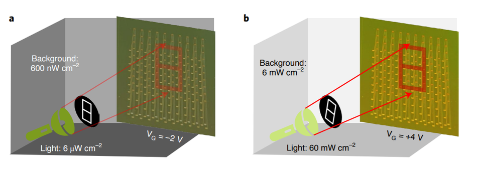
After understanding the light-intensity-dependent and time-dependent characteristics of the MoS2 phototransistors, the team evaluated the sensing and adaptation functions in the human retina with MoS2 phototransistor arrays. With the help of an 8x8 device array to perceive a pattern of 8, for the scotopic adaptation test, the pixel array is subject to a dark background of 600nW/cm2 to recognize a low-intensity image of 6uW/cm2. In the case of the photopic adaptation test, the pixel array is under a bright background of 6mW/cm2 to perceive a strong-light image of 60mW/cm2.

To evaluate the scope of visual adaptation for image recognition applications, the team built a vision system consisting of an adaptive MoS2 phototransistor array with a three-layer artificial neural network (ANN). The team uses the MNIST dataset as a training set to determine the accuracy of image recognition in a normal environment. The above image shows the adaptation process of the MoS2 phototransistor to capture and perceive the pattern. It can be seen that the accuracy of scotopic adaptation is sharp, signifying the quick adaptation to the surrounding light intensity, while in photopic adaptation, the phototransistor takes quite some time to provide maximum accuracy. In scotopic adaptation, the maximum accuracy reached is 97% at 40 seconds from 38.6% at 2 seconds, and in photopic adaption, the accuracy improves from 9.5% at 2 seconds to 96.1% at 80 seconds.
The research article reports a visual sensor array that uses button-gate bilayer MoS2 phototransistor configuration to emulate the visual adaptation functions in the retina. “This bioinspired in-sensor adaptation strategy can widen the range for image perception under different illumination conditions, which simplify the complexity of hardware and algorithms and enhance the functionalities for processing images at sensory terminals,” the team notes. “Our MoS2 phototransistor arrays exhibit both scotopic and photopic adaptations, offering a broad perception range and image contrast enhancement.”
The research paper was published in Nature Electronics on February 3, 2022, under closed-access terms.
Resources
Liao, F., Zhou, Z., Kim, B.J. et al. Bioinspired in-sensor visual adaptation for accurate perception. Nat Electron (2022). https://doi.org/10.1038/s41928-022-00713-1