What is a Semiconductor? A Comprehensive Guide to Engineering Principles and Applications
Semiconductors are the building blocks of modern electronics, powering everything from smartphones to satellites. This in-depth guide provides a comprehensive understanding of semiconductors' engineering principles and applications, delving into their fundamental concepts, materials, devices, manufacturing processes, and their impact on today's technology landscape.

20 Jul, 2023. 20 minutes read
Semiconductor Technology
Introduction
Semiconductors are materials that have electrical conductivity between that of a conductor and an insulator. They're often made from silicon, germanium, or other materials that have four valence electrons in their outermost shell, often called tetravalent materials. Tetravalent materials are ideal for use in semiconductors because they can form covalent bonds with other tetravalent materials, creating a stable lattice structure that allows for controlled electrical conductivity.
Therefore, by adding impurities, either trivalent or pentavalent materials to these tetravalent materials, engineers can create semiconductors with specific electrical properties that make them ideal for use in electronic devices. These impurities that are added to semiconductors to create specific electrical properties are called dopants. Common dopants are Boron, Phosphorus, Arsenic, Antimony, Aluminum, Gallium, Indium, and many others. Engineers can produce semiconductors with specific features that are perfect for use in electronic devices because each of these dopants has a unique impact on the electrical properties of the semiconductor.
Semiconductors have revolutionized the world of electronics, making it possible to create smaller, faster, and more powerful devices. They play a crucial role in modern technology, as they form the basis of electronic devices such as transistors, diodes, and integrated circuits. They're used in everything from microchips and processors to solar panels and LED lights. Understanding how semiconductors work is critical for anyone interested in electronics.[1]
Further reading: Chips and Wafers: Making of the semiconductor industry
Basics of Semiconductors
Semiconductors are materials that exhibit electrical properties between those of conductors, which allow the free flow of electric current, and insulators, which resist the flow of electric current. The unique properties of semiconductors arise from their atomic structure and the arrangement of their electrons in energy bands. In semiconductors, the valence band, which contains the outermost electrons, is separated from the conduction band, where electrons can move freely, by a relatively small energy gap called the band gap.
The temperature, impurities, or application of an electric field are all ways to modify the conductivity in semiconductors. Semiconductors may be designed to perform various tasks, including signal amplification, switching between on and off states, and transferring energy from one form to another, making them the perfect building blocks for electronic devices.
Intrinsic and Extrinsic Semiconductors
Semiconductors can be classified into two types: intrinsic and extrinsic. Intrinsic semiconductors are pure materials with no added impurities, and their electrical properties are solely determined by the material's inherent characteristics. Intrinsic semiconductors have a limited number of charge carriers, which are generated by thermal energy. As a result, their conductivity is relatively low and highly dependent on temperature.
Extrinsic semiconductors, on the other hand, are created by introducing impurities into the intrinsic material through a process called doping. Doping involves adding a small amount of another element, called a dopant, to the semiconductor material. The dopant atoms have either more or fewer valence electrons than the semiconductor atoms, resulting in excess or deficiency of charge carriers.
There are two types of extrinsic semiconductors: n-type and p-type. In n-type semiconductors, the dopant atoms have more valence electrons than the semiconductor atoms, resulting in an excess of negatively charged electrons. Conversely, in p-type semiconductors, the dopant atoms have fewer valence electrons than the semiconductor atoms, creating an excess of positively charged "holes." The ability to control the type and concentration of charge carriers in extrinsic semiconductors allows engineers to design electronic devices with specific characteristics and functionalities. Trivalent dopants such as boron or aluminum are commonly used to create p-type semiconductors, while pentavalent dopants such as phosphorus or arsenic are commonly used to create n-type semiconductors.
Energy Bands and Band Gap
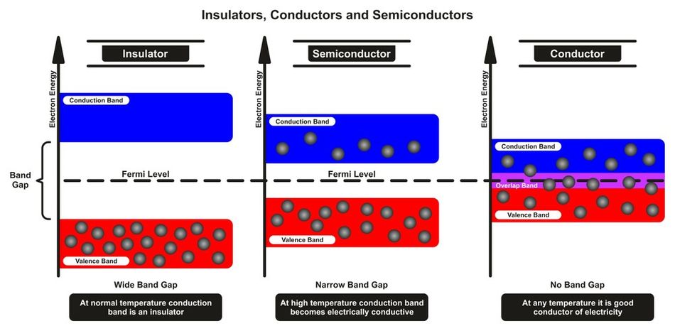
In semiconductors, the arrangement of electrons in energy levels plays a crucial role in determining their electrical properties. Electrons in a semiconductor occupy specific energy bands, which are continuous ranges of energy levels that electrons can have within the material. The two most important energy bands in semiconductors are the valence band and the conduction band.
The valence band is the highest energy band that is fully occupied by electrons at an absolute zero temperature. These electrons are tightly bound to their parent atoms and are responsible for forming chemical bonds between atoms. As the temperature increases, some of these electrons gain enough energy to break free from their parent atoms and move to the conduction band.
The conduction band is the next higher energy band above the valence band, and it is partially or totally empty at an absolute zero temperature. Electrons in the conduction band are free to move within the material, allowing them to participate in the conduction of electric current.
The energy gap between the valence band and the conduction band is called the band gap. It is the energy difference between the top of the valence band and the bottom of the conduction band. It represents the minimum energy required for an electron to transition from the valence band to the conduction band. The size of the band gap is a critical factor in determining the electrical properties of a semiconductor. Materials with a large band gap, typically greater than 3 electron volts (eV), are considered insulators, as their electrons require a significant amount of energy to move to the conduction band. Materials with a small band gap, typically between 0.1 and 3 eV, are classified as semiconductors.
The conductivity of a semiconductor increases with temperature, as more electrons gain enough energy to overcome the band gap and move to the conduction band. In contrast, materials with no band gap, such as metals, are conductors, as their valence and conduction bands overlap, allowing electrons to move freely and conduct electric current. So, for a semiconductor to conduct electricity, electrons must be able to move from the valence band to the conduction band by acquiring enough energy to overcome the band gap. The ability to control the movement of electrons between the valence and conduction bands is what makes semiconductors so useful in electronic devices.[2]
Semiconductor, Pure Semiconductor, and Pure Elements
Pure elements are not semiconductors because they have a filled valence band and an empty conduction band, which means that they do not have the electrical properties necessary to perform as a semiconductor. For a material to be a semiconductor, it must have a partially filled valence band and an empty conduction band. This allows electrons to move from the valence band to the conduction band when energy is applied to the material, which is necessary for the material to conduct electricity.
Pure elements such as copper, aluminum, and gold are examples of materials that are not semiconductors. However, some pure elements such as silicon and germanium can be doped to create semiconductors. When a small amount of impurity is added to the pure element, it can create a region of the material with different electrical properties. This is useful for creating p-type and n-type semiconductors, which are necessary for creating electronic devices such as transistors and integrated circuits. Pure semiconductors, such as intrinsic silicon or germanium, are semiconductors that have not been intentionally doped with impurities. These materials have a partially filled valence band and an empty conduction band, which allows them to conduct electricity but not as efficiently as doped semiconductors.
Intrinsic semiconductors are useful for studying the fundamental properties of semiconductors and for creating devices such as photodiodes and radiation detectors. However, they are not as commonly used in electronic devices as doped semiconductors because they do not have the electrical properties necessary to perform as well as doped semiconductors.
Semiconductor Materials
A crucial component of electrical device design is choosing the right semiconductor material for the right application. The choice of material depends on factors such as the desired electrical properties, thermal stability, and fabrication compatibility. Some of the most commonly used semiconductor materials include silicon, germanium, and compound semiconductors such as gallium arsenide and indium phosphide. When designing electrical equipment, it is important to take into account the advantages and disadvantages of each of these materials.
Silicon(Si)
Silicon is the most widely used semiconductor material, accounting for more than 90% of the global semiconductor market. Its popularity can be attributed to several factors, including its abundant availability, as it is the second most abundant element in the Earth's crust. Silicon also has a relatively large band gap of 1.12 eV, which provides a good balance between electrical conductivity and thermal stability.
One of the key advantages of silicon is its excellent thermal properties. Silicon has a high melting point (1,414°C) and a low thermal expansion coefficient, which allows it to maintain its structural integrity and electrical performance over a wide temperature range. This makes silicon an ideal material for high-temperature applications, such as power electronics and automotive systems. The unique electronic properties of silicon are due to its ability to form covalent bonds with other elements, which allows it to create stable lattice structures often referred to as silicon crystals.
Silicon also benefits from a well-established manufacturing infrastructure, which has been developed and refined over several decades. The mature silicon fabrication technology enables the production of high-quality, reliable, and cost-effective semiconductor devices. Some common silicon-based devices include metal-oxide-semiconductor field-effect transistors (MOSFETs), bipolar junction transistors (BJTs), and silicon-based solar cells.
However, silicon is not without its limitations. For example, it has relatively low electron mobility compared to other semiconductor materials, which can limit the performance of high-speed electronic devices. Additionally, silicon is an indirect bandgap material, which makes it less efficient for light-emitting applications, such as light-emitting diodes (LEDs) and laser diodes.
Germanium(Ge)
Germanium is another important semiconductor material, although it is less commonly used than silicon. Germanium was the first material used to create transistors in the early days of semiconductor technology, but it was later replaced by silicon due to its superior thermal properties and abundant availability. However, germanium still has some unique properties that make it an attractive choice for certain applications.
One of the key advantages of germanium is its high electron mobility, which is approximately three times higher than that of silicon. This property allows germanium-based devices to operate at higher speeds, making them suitable for high-frequency applications such as radio frequency (RF) communication systems and high-speed digital circuits.
Germanium also has a smaller band gap (0.66 eV) compared to silicon, which results in a higher intrinsic carrier concentration at room temperature. This property can be advantageous for certain applications, such as infrared (IR) detectors and thermoelectric devices, where a higher carrier concentration is desirable.
However, germanium has some drawbacks that limit its widespread use in semiconductor devices. One of the main challenges is its poor thermal stability, as germanium has a lower melting point (937°C) and a higher thermal expansion coefficient than silicon. This makes germanium-based devices more susceptible to thermal degradation and limits their use in high-temperature applications.
Another limitation of germanium is its higher cost compared to silicon, due to its lower natural abundance and more complex manufacturing processes. Despite these challenges, germanium remains an important semiconductor material for specialized applications, such as high-speed transistors, infrared detectors, and advanced solar cells.[3]
Further reading: Silicon Wafers: Everything You Need to Know
Compound Semiconductors
Compound semiconductors are materials composed of two or more elements from different groups in the periodic table. Compound semiconductors are materials that are made up of two or more elements from different groups of the periodic table. These materials have unique electrical and optical properties that make them useful in a wide range of electronic and optoelectronic applications.
Compound semiconductors are typically made using a process called epitaxy, which involves growing a thin layer of the compound semiconductor material on top of a substrate material. The epitaxial growth process allows engineers to create compound semiconductor materials with precise properties and structures. Unlike elemental semiconductors, such as silicon and germanium, compound semiconductors exhibit a wide range of electrical, optical, and thermal properties, making them suitable for a variety of specialized applications.
Some common compound semiconductors include gallium arsenide (GaAs), indium phosphide (InP), and gallium nitride (GaN). They have a wide range of electrical and optical properties, and they can be doped to create regions of the material with different electrical properties. These materials offer several advantages over elemental semiconductors, such as higher electron mobility, direct bandgap, and improved thermal stability.
Gallium arsenide (GaAs) is a compound semiconductor with a band gap of 1.43 eV, which is larger than that of silicon. GaAs has a higher electron mobility than silicon, allowing for faster response times and higher-frequency operation. This makes GaAs an ideal material for high-speed electronic devices, such as radio frequency (RF) and high-power microwave devices, as well as optoelectronic devices, such as LEDs and laser diodes. However, GaAs is more expensive and less abundant than silicon, which can limit its widespread adoption.
Indium phosphide (InP) has a bandgap of 1.35 eV and exhibits even higher electron mobility than GaAs. InP is particularly well-suited for high-speed optoelectronic devices, such as photodetectors and high-speed transistors, due to its direct bandgap and excellent electron transport properties. InP is also used as a substrate material for the epitaxial growth of other compound semiconductors, such as indium gallium arsenide (InGaAs) and indium gallium phosphide (InGaP).
Gallium nitride (GaN) is a wide bandgap semiconductor with a bandgap of 3.4 eV, making it suitable for high-power and high-temperature applications. GaN has excellent thermal stability and high breakdown voltage, which enables the development of high-power electronic devices, such as power transistors and high-brightness LEDs. GaN-based devices are also known for their high efficiency and long operational lifetimes, making them attractive for energy-efficient lighting and power conversion systems.
The choice of a compound semiconductor material depends on the specific requirements of the application, such as the desired electrical, optical, and thermal properties, as well as the compatibility with existing manufacturing processes. By leveraging the unique advantages of compound semiconductors, engineers can develop innovative electronic devices with enhanced performance and functionality.[4]
Further reading: How are Semiconductors Made? A Comprehensive Guide to Semiconductor Manufacturing
Semiconductor Devices
Semiconductor devices are the building blocks of modern electronic systems, enabling the manipulation and control of electrical signals in a wide range of applications. These devices use the special capabilities of semiconductors to carry out a variety of tasks, including signal amplification, switching between on and off states, and energy conversion. Diodes, transistors, and integrated circuits are some of the most popular semiconductor devices, and each has a unique set of operating principles and applications.
Diodes
Diodes are semiconductor devices that allow an electric current to flow in one direction while blocking it in the opposite direction. They consist of a junction formed by two layers of semiconductor material, one n-type and one p-type. When a positive voltage is applied to the n-type layer and a negative voltage to the p-type layer, the diode is said to be forward-biased, and current flows through the junction. Conversely, when the voltage polarity is reversed, the diode is reverse-biased, and the current flow is blocked.
Diodes have a wide range of applications in electronic circuits, including rectification, voltage regulation, and signal modulation. Rectification is the process of converting alternating current (AC) to direct current (DC), which is essential for powering electronic devices that require a stable DC voltage. Voltage regulation involves maintaining a constant output voltage despite variations in input voltage or load current, ensuring the proper operation of sensitive electronic components. Signal modulation is the process of modifying a signal's characteristics, such as its amplitude or frequency, to transmit information or control other devices.
There are several types of diodes, each with its specific characteristics and applications. Some common types include rectifier diodes, Zener diodes, Schottky diodes, and light-emitting diodes (LEDs). Rectifier diodes are used for converting AC to DC, while Zener diodes are designed to maintain a constant voltage across their terminals when reverse-biased. Schottky diodes have a lower forward voltage drop and faster switching speeds than conventional diodes, making them suitable for high-frequency applications. LEDs emit light when forward-biased, enabling their use in various lighting and display applications.
Transistors
Transistors are semiconductor devices that can be used to amplify or switch electronic signals. They are the fundamental building blocks of modern electronic circuits and are found in various applications, from simple amplifiers to complex integrated circuits. Transistors consist of three layers of semiconductor material, with alternating n-type and p-type layers, forming either an n-p-n or a p-n-p configuration.
There are two main types of transistors: bipolar junction transistors (BJTs) and field-effect transistors (FETs). Both types of transistors have three terminals: the emitter (E) and collector (C) for BJTs, and the source (S) and drain (D) for FETs. The third terminal called the base (B) in BJTs and the gate (G) in FETs, is used to control the flow of current between the other two terminals.
Bipolar junction transistors (BJTs) operate by using a small current at the base terminal to control a larger current between the emitter and collector terminals. In an n-p-n BJT, a small forward-biased current flows from the base to the emitter, allowing a larger current to flow from the collector to the emitter. Conversely, in a p-n-p BJT, a small forward-biased current flows from the emitter to the base, allowing a larger current to flow from the emitter to the collector. BJTs can be used as amplifiers, switches, or in more complex configurations, such as oscillators and multivibrators.
Further reading: NPN vs PNP BJT Transistor: Understanding the basics
Field-effect transistors (FETs) operate by using a voltage applied to the gate terminal to control the current between the source and drain terminals. There are two main types of FETs: junction field-effect transistors (JFETs) and metal-oxide-semiconductor field-effect transistors (MOSFETs). In both types, the gate voltage controls the conductivity of a channel between the source and drain terminals, allowing or blocking the flow of current. FETs are widely used in electronic circuits due to their high input impedance, low power consumption, and fast switching speeds. They are commonly found in applications such as amplifiers, switches, and digital logic circuits.
Transistors have revolutionized the field of electronics, enabling the development of increasingly complex and powerful electronic devices. By understanding the operation principles and applications of transistors, engineers can design and build a wide range of electronic systems, from simple analog circuits to advanced digital systems.[5]
Further reading: PMOS VS NMOS: Focus on Two Main Forms of MOSFET
Integrated Circuits
Integrated circuits (ICs) are semiconductor devices that contain multiple electronic components, such as transistors, diodes, resistors, and capacitors, fabricated on a single piece of semiconductor material, typically silicon. The integration of multiple components on a single chip enables the creation of complex electronic systems with reduced size, weight, and power consumption compared to discrete component assemblies. ICs are the foundation of modern electronic devices, including computers, smartphones, and various consumer electronics.
The basic operation of an integrated circuit involves the interaction of its various components to process, store, or transmit electrical signals. The components are interconnected through a network of conductive pathways, called interconnects, which are formed on the semiconductor substrate during the fabrication process. The layout and design of the components and interconnects determine the functionality and performance of the integrated circuit.
There are several types of integrated circuits, each designed for specific applications and functions. Some common types include digital ICs, analog ICs, and mixed-signal ICs. Digital ICs process binary signals, such as those used in digital computers and communication systems. Examples of digital ICs include microprocessors, memory chips, and logic gates. Analog ICs process continuous signals, such as those found in audio and video systems. Examples of analog ICs include operational amplifiers, voltage regulators, and analog-to-digital converters. Mixed-signal ICs combine both digital and analog functions on a single chip, enabling the processing of both continuous and discrete signals. Examples of mixed-signal ICs include data converters, radio frequency (RF) transceivers, and system-on-chip (SoC) devices.
The development of integrated circuits has followed a trend known as Moore's Law, which states that the number of transistors on a chip doubles approximately every two years. This exponential growth in transistor density has enabled the creation of increasingly powerful and complex electronic systems, driving advancements in computing, communication, and consumer electronics. However, as the size of transistors approaches the atomic scale, new challenges and limitations arise, such as increased power consumption, heat generation, and manufacturing complexity. These challenges are driving the development of new materials, device architectures, and fabrication techniques to continue the evolution of integrated circuit technology.[6]
Further reading: Types of IC Packages: A Comprehensive Guide
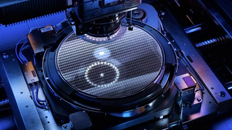
Semiconductor Manufacturing
The process of manufacturing semiconductor devices involves a series of complex and precise steps to create the desired electronic components on a semiconductor substrate, such as silicon or gallium arsenide. These steps include material preparation, patterning, etching, deposition, doping, and packaging, among others. Each stage of the manufacturing process requires careful control of parameters such as temperature, pressure, and chemical composition to ensure the production of high-quality, reliable, and cost-effective devices.
Photolithography
Photolithography is a critical step in the semiconductor manufacturing process, as it enables the transfer of intricate patterns onto the semiconductor substrate. The process involves the use of light-sensitive materials called photoresists, which are applied to the substrate as a thin film. A mask containing the desired pattern is then placed over the photoresist, and the assembly is exposed to ultraviolet (UV) light. The exposed areas of the photoresist undergo a chemical reaction, making them either more or less soluble in a developer solution, depending on the type of photoresist used.
After exposure, the substrate is immersed in the developer solution, which selectively removes the exposed or unexposed regions of the photoresist, revealing the underlying substrate in the patterned areas. The exposed substrate can then be subjected to further processing steps, such as etching or deposition, to create the desired semiconductor structures.
Photolithography technology has evolved significantly over the years, with advancements in mask design, light sources, and photoresist materials enabling the production of increasingly smaller and more complex semiconductor devices. However, as device dimensions continue to shrink, new challenges arise, such as the need for higher-resolution patterning techniques and improved process control to maintain the quality and performance of the resulting devices.
Etching and Deposition
Etching and deposition are two critical processes in semiconductor manufacturing that involve removing and adding material layers, respectively. These processes are essential for defining the intricate patterns and structures of semiconductor devices, such as transistors and integrated circuits.
Etching is the process of selectively removing material from a semiconductor substrate or layer to create the desired pattern or structure. There are two main types of etching techniques: wet etching and dry etching. Wet etching involves immersing the semiconductor material in a chemical solution that reacts with the material, selectively dissolving it to create the desired pattern. Wet etching is typically isotropic, meaning that it etches in all directions, which can limit its ability to create high-resolution features. However, it is a relatively simple and low-cost process, making it suitable for certain applications.
Dry etching, on the other hand, uses a reactive gas or plasma to remove material from the semiconductor surface. There are several dry etching techniques, including reactive ion etching (RIE), deep reactive ion etching (DRIE), and plasma etching. Dry etching processes are generally anisotropic, meaning that they etch in a single direction, which allows for the creation of high-resolution features and complex structures. However, dry etching techniques can be more complex and expensive than wet etching methods.
Deposition is the process of adding material layers to a semiconductor substrate, either by growing the material directly on the substrate or by depositing it from a gas or liquid phase. There are several deposition techniques, including chemical vapor deposition (CVD), physical vapor deposition (PVD), and atomic layer deposition (ALD).
Chemical vapor deposition (CVD) involves the reaction of gaseous precursors on the semiconductor surface, resulting in the formation of a solid material layer. CVD can produce high-quality, uniform films with good adhesion and conformality, making it a popular choice for many semiconductor applications. However, CVD processes often require high temperatures and can produce unwanted byproducts, which can be challenging to manage.
Physical vapor deposition (PVD) uses physical processes, such as evaporation or sputtering, to deposit material layers onto the semiconductor substrate. PVD techniques are typically less expensive and more versatile than CVD methods, but they can produce less uniform and conformal films.
Atomic layer deposition (ALD) is a more recent deposition technique that involves the sequential exposure of the substrate to gaseous precursors, resulting in the formation of a single atomic layer per cycle. ALD offers excellent control over film thickness and uniformity, as well as the ability to deposit conformal films on high-aspect-ratio structures. However, ALD processes can be slow and more expensive than other deposition methods.
The choice of etching and deposition techniques depends on the specific requirements of the semiconductor device, such as the desired feature size, material properties, and manufacturing cost. By carefully selecting and optimizing these processes, semiconductor manufacturers can create high-performance, reliable, and cost-effective devices.[7]
Further reading: Dry Etching vs Wet Etching: Everything You Need To Know
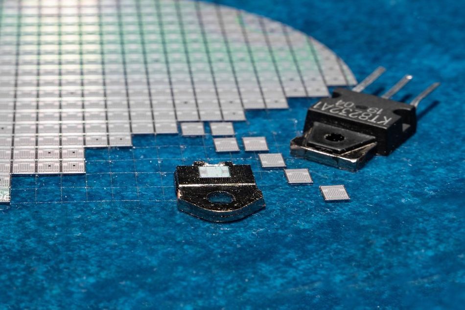
Packaging and Testing
Packaging and testing are critical steps in the semiconductor manufacturing process, ensuring the functionality, reliability, and performance of the final product. Packaging involves enclosing the semiconductor die, which contains the active electronic components, in a protective casing that provides electrical connections, mechanical support, and thermal management. Testing involves verifying the electrical performance of the packaged device and identifying any defects or failures that may have occurred during the manufacturing process.
Packaging plays a crucial role in protecting semiconductor devices from environmental factors, such as moisture, dust, and mechanical stress, while also facilitating electrical connections to external circuits. There are several types of semiconductor packages, each with its own set of advantages and trade-offs. Some common package types include dual in-line packages (DIPs), small-outline integrated circuits (SOICs), and ball grid arrays (BGAs). DIPs are an older package type with through-hole mounting, while SOICs and BGAs are surface-mount packages that offer higher component density and improved electrical performance.
Thermal management is another important aspect of packaging, as semiconductor devices generate heat during operation, which can affect their performance and reliability. Efficient heat dissipation is essential to prevent overheating and ensure the long-term stability of the device. Various techniques are used to manage heat in semiconductor packages, such as heat sinks, thermal vias, and thermal interface materials.
Testing is a critical step in the semiconductor manufacturing process, as it ensures that the final product meets the required performance specifications and is free of defects. Semiconductor testing involves applying electrical signals to the device under test (DUT) and measuring its response to verify its functionality and performance. This process can identify manufacturing defects, such as short circuits, open circuits, and incorrect component values, as well as performance issues, such as excessive power consumption or poor signal integrity.
Testing can be performed at various stages of the manufacturing process, including wafer-level testing, package-level testing, and final system-level testing. Wafer-level testing is performed on the semiconductor die before it is separated from the wafer and packaged, while package-level testing is performed on the fully packaged device. System-level testing involves testing the semiconductor device within its final application environment, ensuring that it functions correctly in real-world conditions.
The complexity and cost of semiconductor testing can vary depending on the type of device, its performance requirements, and the specific test methodologies employed. Advanced testing techniques, such as built-in self-test (BIST) and design-for-testability (DFT) strategies, can help reduce test complexity and improve test coverage, ensuring the highest possible product quality and reliability.[8]
Further reading: PCB Manufacturing Process: Everything You Need to Know
Conclusion
In this guide, we have explored the fundamental concepts, materials, devices, and manufacturing processes related to semiconductors. By understanding the engineering principles and applications of semiconductors, you can appreciate their critical role in modern technology and their impact on various industries. As semiconductor technology continues to evolve, new materials, devices, and fabrication techniques will drive advancements in electronic systems, enabling the development of increasingly powerful and efficient devices that shape our daily lives.
Frequently Asked Questions
1. What is the difference between a conductor, an insulator, and a semiconductor?
A conductor is a material that allows the free flow of electric current due to the presence of a large number of free charge carriers. An insulator is a material that resists the flow of electric current due to the absence of free charge carriers. A semiconductor is a material with electrical properties between those of conductors and insulators, and its conductivity can be controlled by altering its temperature, impurities, or the application of an electric field.
2. What are the main types of semiconductors?
Semiconductors can be classified into two types: intrinsic and extrinsic. Intrinsic semiconductors are pure materials with no added impurities, while extrinsic semiconductors are created by introducing impurities into the intrinsic material through doping.
3. What is the role of the band gap in semiconductors?
The band gap is the energy difference between the top of the valence band and the bottom of the conduction band in a semiconductor. It represents the minimum energy required for an electron to transition from the valence band to the conduction band. The size of the band gap is a critical factor in determining the electrical properties of a semiconductor.
4. What are some common semiconductor materials and their applications?
Some common semiconductor materials include silicon, germanium, and compound semiconductors such as gallium arsenide and indium phosphide. Silicon is the most widely used semiconductor material and is found in devices such as transistors, diodes, and integrated circuits. Germanium is used in high-speed electronic devices, while compound semiconductors are used in specialized applications such as high-frequency communication systems and optoelectronic devices.
5. What are the main types of semiconductor devices and their functions?
Some common semiconductor devices include diodes, transistors, and integrated circuits. Diodes allow an electric current to flow in one direction while blocking it in the opposite direction. Transistors can be used to amplify or switch electronic signals. Integrated circuits contain multiple electronic components on a single chip, enabling the creation of complex electronic systems with reduced size, weight, and power consumption.
Reference
Semiconductors Industry Association, 2023. Semiconductors are the Brains of Modern Electronics. Available at: https://www.semiconductors.org/semiconductors-101/what-is-a-semiconductor/ (Accessed: July 10, 2023).
BYJU’S, 2019. Definition and Classification of Energy Bands | Band Theory. Available at: https://byjus.com/physics/what-are-energy-bands/ (Accessed: July 10, 2023).
Herres, D. (Test and Measurement Tips), 2016. Why silicon and germanium are semiconductors. Available at: https://www.testandmeasurementtips.com/why-silicon-and-germanium-are-semiconductors/#:~:text=Silicon%2Dgermanium%20serves%20as%20a,regions%20of%20dissimilar%20crystalline%20semiconductors. (Accessed: July 11, 2023).
Abbasi, I., 2022. A Close Analysis of Compound Semiconductors. Available at: https://www.azom.com/article.aspx?ArticleID=21555 (Accessed: July 11, 2023).
Saini, M.K., 2022. Difference between Diode and Transistor. Available at: https://www.tutorialspoint.com/difference-between-diode-and-transistor (Accessed: July 11, 2023).
Charig, N., 2022. What are integrated circuits? Definition, types, and more. Available at: https://www.power-and-beyond.com/what-are-integrated-circuits-definition-types-and-more-a-66046a289105d037a11ba94461ef9c5e/ (Accessed: July 11, 2023).
Ayodele, A.(Wevolver), 2023. Thin Film Deposition: Everything You Need to Know. Available at: https://www.wevolver.com/article/thin-film-deposition-everything-you-need-to-know (Accessed: July 11, 2023).
Rao, R.(Wevolver), 2023. Semiconductor Resilience with Innovations in Testing Techniques and Packaging. Available at: https://www.wevolver.com/article/semiconductor-resilience-with-innovations-in-testing-techniques-and-packaging (Accessed: July 11, 2023).