Bare Board Technology: Everything You Need to Know
Bare boards are the skeletal framework of printed circuit boards (PCBs). They are without electrical components which should have made it a fully functional PCB. This article details the uses, benefits, and drawbacks of bare boards, including the types of bare board testing.

Last updated on 23 Jul, 2024. 24 minutes read
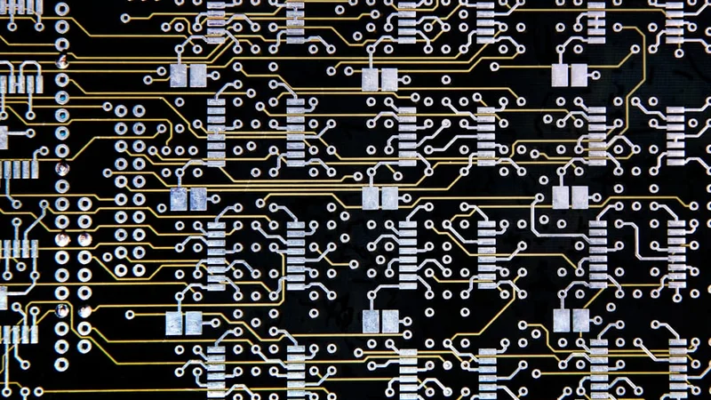
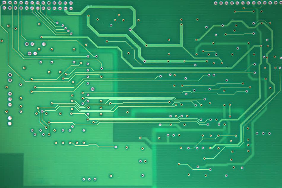
Bare printed circuit board
Introduction
The bare printed circuit board is the foundational component of a printed circuit board, upon which other surface mounts or SMT components such as resistors, capacitors, and integrated circuits are mounted and connected. The relative emptiness of the board allows technicians to conduct several tests to ensure suitability to the desired PCB design, and proactively correct errors where necessary.
A bare PCB typically consists of a flat, non-conductive substrate, commonly made from materials like FR4 (a fiberglass-reinforced epoxy laminate), which provides structural support. Thin layers of copper foil are laminated onto this substrate to form conductive pathways that interconnect different components. These unpopulated boards are meticulously crafted, often involving multiple layers to accommodate complex circuitry and increased functionality.
With advances in miniaturization and multi-layer PCB designs, modern bare PCBs cater to the demands of high-density applications, driving innovation in industries from consumer electronics to automotive systems and telecommunications.
Bare boards are crucial in today's technology, impacting devices from smartphones to modern vehicles. Their quality and design are essential for reliable and high-performance operation, underpinning the seamless functioning of countless electronic systems in our daily lives.
Understanding Bare Boards: The Basics
What is a Bare Board?
A bare board PCB refers to a printed circuit board that is devoid of electronic components. It is the skeleton of the conventional PCB before it is populated. Constructed from a non-conductive substrate, typically FR4, a fiberglass-reinforced epoxy laminate, a bare board includes metal coating, conductive pathways, and patterns. It undergoes photo-resist lamination, etching, drilling, solder mask application, and silkscreen printing.
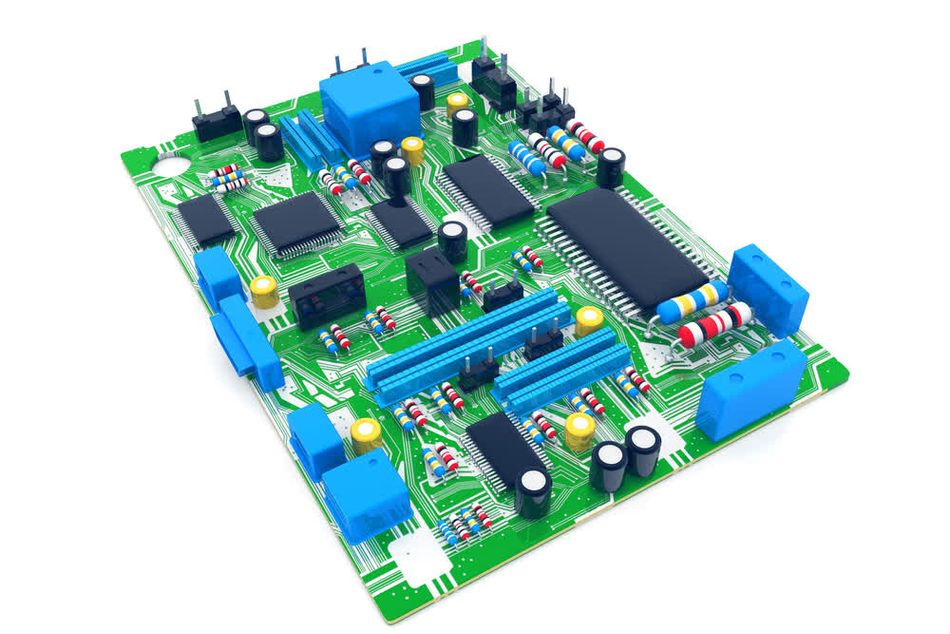
In the industry, bare boards are also known as bare PCBs, blank PCBs, or simply PCBs, while an assembled board is referred to as a PCB assembly (PCBA).
Bare boards provide electrical and mechanical support for circuit production. They offer flexibility and versatility, making them viable for mass production. Modern bare boards range from simple single-layer configurations to complex multi-layer structures, essential for high-density electronic systems. Advanced manufacturing techniques such as laser direct structuring and microvia drilling have further refined the precision and capability of modern bare boards, ensuring their critical role in applications from consumer electronics to aerospace systems.
Industry standards, particularly IPC-2221, provide comprehensive guidelines to ensure consistency in design, fabrication, and quality assurance, fostering the reliability and performance essential in today’s technology landscape.
Recommended reading: PWB vs PCB: Differences and Similarities
Essential Components of Bare Boards
Every intricate PCB originates from a basic bare board. Despite its modest name, this foundational element plays a critical role, housing essential components that underpin sophisticated electronic devices. Here are the fundamental components that constitute the essence of a bare board:
Substrate: The foundation that provides mechanical support and electrical insulation. Made from materials like FR4 (fiberglass & epoxy laminate) for balance of strength and heat resistance. Specialized applications may use polyimide (flexible & heat-resistant) or ceramic composites (excellent thermal conductors).
Copper Traces: The highways, forming conductive pathways for electrical signals. Etched onto the substrate for precise connections. Width and thickness determine current capacity and signal integrity. Advancements allow finer traces for miniaturization and improved performance.
Vias: The bridges, connecting different layers in multi-layer PCBs for complex interconnections. Types include:
Through-hole vias: Drilled through the entire board for strong connections.
Blind vias: Connect outer layers to inner layers without penetrating the board.
Buried vias: Exist entirely within internal layers. Materials like copper plating ensure reliable connections across layers for compact and functional PCBs. Advancements in via technology (laser drilling, plating methods) enhance capabilities for greater design flexibility and performance.
Recommended reading: PCB Via: What is a Via?
When to Use a Bare Board
Bare boards are designed to be configured, so they can be used to test its design, concept, and functionality before more expensive components are assembled to make a PCB. These bare boards offer mechanical support to the components, traces, and pads as they are the substrates that house all other components. This means that bare boards are a foundational element, essential for PCB fabrication and design, and by extension, electronics production.
The bare board is useful for carrying out testing in order to preempt possible issues that may occur at a later stage of the PCB fabrication process which would affect the usability of an electronic device.
Advantages of Bare Board
The bare PCB board offers a lot of benefits such as the earlier mentioned mechanical support to the components, traces, and pads that are mounted and designed onto the board; more so, the circuit connections on the board allow the routing of electrical current between the components it carries. As the base of all printed circuit board assembly, the bare board is indispensable to PCB fabrication, and has proven advantageous for the following reasons:
Early Detection of Defects: Without components, boards are easier to test and appraise. The board’s layout and surfaces aren’t occupied by electrical components or other obstructions, so they can be examined based on the structure and design. Any issues in the circuitry or selected components can be assessed and rectified before the full circuit is completed.
Cost Saving: The foundational process of board design, testing, and basic fabrication ensures that the board is functional and durable. This gives room for early detection of problems that might be expensive to fix later on, if at all possible. When problems are identified early, erroneous assembly with expensive components can be avoided, thereby reducing the risk of money loss.
Time-Saving: Early prototyping and testing ensures satisfactory and design-specific functionality, so there is no time wasted building a full, but ineffective PCB. Also, the streamlined, automated process compensates for the upfront time investment.
Nevertheless, at any point in board manufacturing, even at the bare board design stage, there is always a chance of accuracy and orientation errors, as well as etching mistakes such as over-etchings, under-etchings, and holes that may cause severe defects. Consequently, thorough inspection is paramount, and the best time to ensure the board is error-free is when it is bare so that mistakes can be intercepted and corrected. This is why bare board testing is important and why bare PCB boards have no real drawback.
What is Bare Board Testing?
Bare board testing is the electrical testing of the unpopulated circuit board to evaluate the continuity and isolation of the board’s connections. The continuity testing process ensures that the circuits have no open points that will hamper the current, while isolation testing determines the resistance between two distinct electrical connections. This test ensures the board circuit's correctness by testing the electrical footprint of the intended design.
When testing is carried out, PCB manufacturers can detect any errors on the bare board early on in the manufacturing process.
Testing bare boards helps to guarantee reliability. PCBs are often densely populated during miniaturization. Therefore, it is vital to ensure that the bare board can solder the expensive components. The slightest error in a blank board will result in an electronic assembly malfunction, being that it is the basis of an electronic system.
Therefore if it fails, the entire system does. This is why the importance of building a good foundation cannot be overstressed.
Bare board testing is especially beneficial in the early stages of board development when it can save the most money and time. By introducing bare board testing into the manufacturing process from the start, many aspects of production can be efficiently streamlined.
Types of Bare Board Testing
The old-fashioned way of testing bare boards is by using a digital multimeter, one connection at a time. However, the complex multilayer board designs of today have phased out such methods to be replaced with more feasible ones suitable for high volume and modern-day production.
Pinned Fixture Test: This is also known as Bed of Nails and In-Circuit testing, and is suitable for large-scale manufacturing. The method tests every connective surface on the PCB board at the same time, using spring-loaded pins or probes. Top and bottom plates apply pressure to a custom pin fixture to ensure a connection across the board. The pinned fixture test is remarkably efficient and only takes a few seconds to complete. It has however shown some downsides such as high expenses and lack of flexibility, because each PCB design requires a new fixture created, together with a custom array of pins.
Flying Probe Test: A flying probe test uses two or more robotic arms equipped with poles that glide across the surface of the board to test each net and verify a PCB’s connections. These flying probe testers travel across the connections using instructions from a software program, checking for opens, shorts, resistance, capacitance, inductance, and diode issues. The flying probe method offers better affordability and flexibility than the pinned fixture test, although it has a longer testing period. This makes it suitable for smaller production quantities where slower testing speed will not restrict the design process.
Automated Optical Inspection (AOI): AOI is a method that applies a single 2D camera or two 3D cameras to photograph the board and compare it to a schematic. If the board doesn’t match the schematic, it can be flagged to undergo visual inspection by a technician. AOI is useful for discovering issues early and altering production plans, but it does not power the board and is not independently fail-safe, so it is usually combined with other testing methods.
Burn-In Test: This type of testing is used to detect failures early and establish the load capacity of the board. This is done by running a power supply through the electronics at an elevated temperature, usually at the highest capacity. This is done continuously for 48 to 168 hours, to eradicate any latent defects activated by the conditions of the test. Due to the intensity of its method, this type of testing can be destructive to the board, but it may spot serious defects before the product is launched.
X-Ray Inspection: This method of testing is used more for board inspection, as radiographs can be used to identify defects like solder connections, barrels, and internal traces, in the early stages of PCB manufacturing. This way, defective elements that may be hidden from the naked eye can be discovered for correction.
Innovations in Bare Board Technology
There are new materials, precision manufacturing techniques, and innovative designs that are pushing the boundaries of what bare boards can accomplish. Consequently, they set the stage for a future of unprecedented electronic performance and reliability.
Advanced Materials and Substrates
As electronics advanced, the demand for better performance in high-frequency and high-temperature environments spurred the development of advanced materials for bare boards. Traditional materials like FR4, while suitable for many applications, often fall short in scenarios requiring superior thermal and electrical properties. This led to the adoption of materials such as Rogers, Taconic, and ceramic substrates, each offering unique advantages tailored to specific needs.
Rogers material is renowned for its outstanding high-frequency performance, originating from the telecommunications industry. These substrates feature a low dielectric constant and low dissipation factor, essential for maintaining signal integrity at high speeds. They are ideal for radar systems, satellite communications, and advanced wireless technologies. However, their superior performance comes with a higher cost, making them suitable for applications where performance is prioritized over expense.
Similarly, Taconic materials are notable for their high-frequency capabilities. These polytetrafluoroethylene PTFE-based laminates offer exceptional thermal stability and low dielectric constant, making them ideal for aerospace and sophisticated telecommunication systems. Taconic laminates withstand extreme thermal conditions, ensuring reliability and performance over a wide temperature range. Their processing demands specialized techniques due to their PTFE composition, but the benefits often outweigh these challenges in highly specialized applications.
Ceramic substrates represent another leap in material advancement, celebrated for their excellent thermal conductivity and mechanical resilience. Used extensively in power electronics, these materials help manage heat dissipation in high-power or high-temperature environments. For instance, aluminum oxide and aluminum nitride ceramics are employed in RF and microwave devices and power amplifiers due to their ability to maintain electrical insulation while providing efficient thermal pathways. These substrates handle the rigors of high-density and high-power applications, though their brittleness and processing complexity can be limiting factors.
The evolution and application of these advanced materials underscore their critical role in modern high-performance electronics. Rogers materials are a staple in satellite communication systems where signal clarity is non-negotiable. Taconic substrates are crucial in the avionics sector, where reliability in extreme conditions is vital. Ceramic substrates ensure that power modules in electric vehicles remain cool and functional, highlighting their indispensable role in emerging technologies.
Comparing these advanced materials, Rogers excels in high-frequency signal transmission, Taconic offers remarkable thermal stability, and ceramics provide unmatched thermal conductivity and mechanical strength. The selection of these materials is driven by specific application requirements, underscoring the tailored solutions they offer for advanced electronic systems.
Understanding the nuances of these advanced substrates—including their benefits, limitations, and ideal applications—allows engineers to make informed decisions, ensuring that the chosen material aligns with the performance demands of their projects. These materials continue to push the boundaries of what electronic systems can achieve, enabling innovations in telecommunications, aerospace, automotive, and beyond. Industry standards, particularly IPC-2221, provide comprehensive guidelines to ensure consistency in design, fabrication, and quality assurance.
Manufacturing Techniques and Methodologies
Traditional PCB manufacturing methods, while effective, often struggle with the demands for higher precision, miniaturization, and complex geometries required by modern electronics. To address these challenges, advanced manufacturing techniques such as additive manufacturing, laser etching, and microvia drilling have been developed and adopted across the industry, bringing remarkable improvements in performance and cost-efficiency.
Additive Manufacturing (AM)
Additive manufacturing, often called 3D printing, disrupts traditional PCB manufacturing by offering a layer-by-layer construction approach. This technique unlocks a new level of design freedom:
Intricate and Customized Designs: Additive manufacturing enables the creation of highly complex geometries impossible with subtractive methods.
Reduced Material Waste: Unlike subtractive methods that remove material, AM minimizes waste, making it a more sustainable option.
Rapid Prototyping: Faster turnaround times for prototypes allow for quicker design iterations and product development cycles.
Emerging in the early 2000s, Additive Manufacturing for PCBs has seen rapid advancements. The aerospace industry exemplifies its benefits by using 3D-printed PCBs for:
Lightweight Components: AM allows for intricate, lightweight structures ideal for weight-sensitive applications.
High-Precision Manufacturing: AM ensures precise feature creation, meeting the strict regulatory standards of the aerospace industry.
Laser Etching
Laser etching, particularly the advanced technique of laser direct structuring (LDS), has transformed the creation of intricate circuits on PCBs. Introduced in the 1990s, it uses high-powered lasers for unmatched accuracy:
Unparalleled Precision: Lasers carve out fine traces and complex patterns with a level of detail impossible with traditional etching methods.
Birth of LDS: Taking it a step further, LDS enables the creation of 3D structures within the PCB itself.
Microvia
Traditional drilling methods struggle to keep pace with the miniaturization demands of modern electronics. Microvia drilling tackles this challenge head-on, enabling high-density interconnections within multi-layer PCBs.
Here's what makes microvia drilling a game-changer:
Laser Power and Plasma Precision: Advancements in laser drilling and plasma etching techniques have enabled the creation of microvias with diameters as small as 50 micrometers – a fraction of the size achievable with traditional methods.
Perfect for Compact Devices: This miniaturization breakthrough is a boon for the manufacture of space-constrained consumer electronics like smartphones and tablets. It allows for more complex circuitry within a limited footprint.
Reliable Connections: The precise nature of laser and plasma drilling ensures highly reliable connections between PCB layers. This translates to optimal performance and long-lasting durability for these devices.
These advanced manufacturing techniques have not only improved precision but also contributed to significant cost reductions. Additive manufacturing minimizes material waste and speeds up the product development cycle, while laser etching and microvia drilling enhance accuracy and enable designs that were previously impossible.
Design Innovations and Trend Tracking
Modern PCB design has undergone a significant transformation, propelled by the need for higher performance and more compact electronic devices. This evolution is rooted in advancing design principles and sophisticated software tools that make the creation of bare boards more efficient and precise.
Historically, PCB design was a labor-intensive process, constrained by manual drafting and basic computer-aided design (CAD) tools. With the rise of consumer electronics in the late 20th century, the demand for smaller, more powerful devices spurred the development of High-Density Interconnect (HDI) technology. HDI allow for more circuitry to be packed within a smaller area through the use of finer lines, smaller vias, and multiple layers. This technology is now a staple in smartphones, tablets, and wearable devices, enabling manufacturers to meet the growing demand for miniaturization without sacrificing functionality.
Simultaneously, the integration of multi-layer PCB designs has addressed the need for more complex circuitry. By stacking several layers of dielectric material and conductive patterns, engineers have been able to significantly increase the number of electrical connections in a given footprint. This innovation is indispensable in applications such as automotive electronics and telecommunications, where space constraints and performance requirements are stringent.
The role of modern design software cannot be understated in facilitating these advancements. Tools like Altium Designer, Autodesk Eagle, and Cadence Allegro have transformed PCB layout processes by offering features that support complex designs. These software platforms provide interactive routing, real-time synchronization, multi-board design capabilities, and robust simulation tools. For example, real-time DRC (Design Rule Check) ensures that designs adhere to manufacturing capabilities and constraints, reducing the risk of costly errors.
In practice, these design tools allow engineers to create intricate HDI and multi-layer PCBs more efficiently. The ability to simulate and validate designs in the software phase ensures that the end products meet the required performance standards before physical prototyping. For instance, in the telecommunications industry, PCB designs must support high data rates and low signal loss, which can be rigorously tested using advanced simulation features.
These innovations profoundly impact manufacturing and the end-use performance of electronic devices. HDI technology improves signal integrity and reduces electromagnetic interference by providing direct and shorter interconnections between components. Multi-layer PCBs enhance electrical performance through better power distribution and signal routing. Such refinements are critical for the development of cutting-edge technologies, from next-gen processors to advanced medical devices.
Incorporating these design principles and leveraging advanced software tools ensure that modern PCBs meet the highest standards of efficiency, reliability, and performance, paving the way for the next wave of technological innovation.
Recommended reading: PCB Layers: Everything You Need to Know
Real-World Applications of Bare Boards in Engineering
Bare boards, though seemingly simple, play a crucial role across various engineering disciplines. Here's a glimpse into their diverse applications:
Automotive Industry
Bare boards, the foundation of PCBs (printed circuit boards), are key players in modern car innovation. They support critical functions like:
Engine Control: Engine control units (ECUs) rely on bare boards to manage fuel, spark timing, and emissions. Special materials ensure these boards function in harsh environments with extreme temperatures and vibrations.
Driver Assistance: Advanced driver-assistance systems (ADAS) use bare boards for real-time data processing from sensors and cameras. Rigorous testing ensures reliable performance in all driving conditions.
Infotainment: Bare boards in infotainment systems handle high-speed data, touchscreens, and external devices. High-density designs allow for miniaturization and complex features.
Thermal Management: Keeping components cool is crucial. Copper heat sinks, thermal vias, and advanced cooling methods prevent overheating and ensure component life. Stringent tests confirm these boards can withstand harsh conditions.
Telecommunications and Networking
Bare boards play a hidden but critical role in telecommunications and networking. They're found within routers, switches, and base stations - the backbone of our modern communication networks. They handle the massive data flow of today's internet, cloud computing, and enterprise networks with ease. Here's how:
High-Speed Highways: They're meticulously crafted to ensure data travels quickly and reliably, like information highways carrying a constant stream of traffic.
Signal Strength: The design ensures signals remain strong and clear, preventing disruptions and dropped connections. This is crucial for smooth network performance.
Routing Efficiency: In routers and switches, bare boards enable the rapid and accurate routing of data packets, making sure information gets where it needs to go quickly and efficiently.
Key Technical Considerations
Here's how bare boards achieve the feat mentioned earlier
Impedance Control: Imagine signal traces as data highways. Impedance control ensures these highways have the "right size" to efficiently carry information. Any mismatch can cause signal reflections, like traffic jams, leading to errors and slowdowns. Precise design, material selection, and manufacturing keep these highways running smoothly.
RF Interference Mitigation: The environment is full of radio frequency noise, potentially disrupting the data flow. Bare boards employ shielding techniques, like a fortress around the data highways, and filters to block unwanted frequencies. These measures keep the signal clear and focused, ensuring reliable data transmission.
High-Frequency Material: Not all materials are created equal for high-speed data. Substrates like Rogers and Taconic are the all-stars. They have minimal signal loss and stable properties, allowing for efficient handling of gigabit data rates – the lifeblood of modern networks.
Practical Applications
In routers and switches, the bare boards are designed to manage high-speed Ethernet interfaces, optical network connections, and other high-frequency signaling paths. They must support technologies such as 10G, 40G, and 100G Ethernet, where maintaining signal integrity and minimizing loss are critical. These requirements necessitate advanced PCB design techniques, including controlled impedance traces and embedded capacitors for signal conditioning.
Base stations, integral to mobile networks, impose even more stringent demands on bare boards. These systems must support multiple frequency bands, and high power outputs, and ensure seamless handoff of mobile signals. The bare boards in base stations utilize complex multi-layer structures to handle the high currents and thermal loads typical of radio frequency (RF) power amplification and signal processing. Advanced thermal management solutions, such as heat sinks and thermal vias, are essential to dissipate heat efficiently and maintain stable operation.
Signal attenuation and jitter are persistent challenges in high-speed data transmission. To mitigate these issues, bare boards in telecommunications hardware often employ differential signaling, which reduces the impact of electromagnetic interference and crosstalk. Additionally, sophisticated signal integrity analysis and simulation during the design phase help identify and address potential issues before fabrication.
The role of bare boards in telecommunications hardware is crucial for ensuring the performance and reliability of network infrastructure. By facilitating high-speed data transmission and robust signal integrity, these components enable the seamless connectivity that powers modern communications.
Consumer Electronics
Bare boards also power the amazing features in your phone, laptop, and even your smartwatch. As electronics shrink and get more powerful, bare board technology has to keep up. Here's how:
Smartphones: Imagine fitting all the parts of a computer into your pocket. That's what high-density interconnect (HDI) technology allows. Bare boards in smartphones use multiple layers stacked together to pack in processors, memory, and more. Tiny connections called microvias keep everything talking smoothly.
Laptops: Laptops need to be both powerful and durable. The main circuit board (motherboard) uses special materials like FR4 to handle heat and keep things running smoothly, even when you're pushing it hard.
Wearables: Flexibility is key for wearables like smartwatches. Special bendy circuit boards made from polyimide allow them to curve and move with you without breaking or glitching.
Challenges and Considerations in Bare Board Technology
While bare boards offer incredible potential, miniaturization, and increasing performance demands present several challenges:
Manufacturing Defects and Quality Assurance
Even tiny flaws in bare boards (PCBs) can cause big problems. Here are some of them and how manufacturers fight them:
Delamination: Imagine the layers of a PCB separating - that's delamination. Weak bonding or heat stress can cause this, leading to weak connections or total failure. Better materials and processes help, but it's a concern for super-important applications like pacemakers.
Shorts: Unintended connections between circuits (like a tiny solder bridge) can cause malfunctions and even damage components. Dense designs with lots of traces make this more likely.
Opens: Missing connections due to broken traces, bad solder joints, or etching errors can render entire circuits useless. In critical applications like spacecraft, this can be disastrous!
So how do manufacturers find and fix these problems? Here are some key tools:
Automated Optical Inspection (AOI): Think of it as a high-tech magnifying glass. AOI uses cameras to scan for visible defects like misaligned parts or missing pieces. Advanced systems even use machine learning to spot hidden issues.
X-ray Inspection: Like an X-ray at the doctor's, this technique sees through the PCB to reveal hidden defects like shorts, opens, and weak solder joints. This is crucial for complex components like Ball Grid Arrays (BGAs). X-ray technology keeps getting better, providing sharper images and faster analysis.
In-Circuit Testing (ICT): This method uses a special fixture to send electrical signals through the PCB, testing each component and connection. It can identify problems like opens, shorts, or even bad components that might be missed by other methods. Modern ICT systems are like super-smart electricians, automatically diagnosing issues.
Reliability and Longevity
For applications like spacecraft, pacemakers, and high-performance cars, bare boards need to be built tough. These devices operate in harsh environments, so ensuring PCB reliability is critical. Here's how manufacturers make sure these boards can withstand the challenges:
Thermal Cycling: Imagine repeatedly heating and freezing a PCB - that's thermal cycling. This simulates extreme temperature changes a board might experience, like the scorching heat of an engine compartment or the frigid vacuum of space. By enduring this test, manufacturers know the board won't crack or fail under real-world conditions.
Vibration Testing: Not everything is smooth sailing! Cars rattle on rough roads, and rockets experience intense vibrations during launch. Vibration testing shakes the PCB to see if anything loosens or breaks. This ensures the board can handle the bumps and vibrations it will encounter during use.
Highly Accelerated Life Testing (HALT): This is like putting a PCB through boot camp! HALT pushes the board to its limits with extreme heat, vibration, and electrical stress. The goal is to find weak spots before they cause problems in the real world. This is especially important for life-critical devices like pacemakers, where failure can have serious consequences.
Beyond these tests, manufacturers also use a technique called Failure Modes and Effects Analysis (FMEA). This involves thinking about every way a board could fail and then taking steps to prevent it. By analyzing each component and connection early in the design phase, FMEA helps identify and address potential issues before they become problems.
Cost Factors and Economical Production
Producing bare boards involves managing numerous cost-related challenges that are essential for achieving economical production. These challenges encompass material costs, manufacturing complexities, chosen techniques, and the benefits of economies of scale. Here's how manufacturers manage the costs:
Material Cost: Standard materials are cost-effective, but high-performance applications might require pricier options like Rogers or Taconic laminates. Manufacturers need to find the right balance between material cost and what the finished product needs to do.
Complexity Counts: More layers, intricate connections (HDI), and tiny vias (microvias) all mean more complex manufacturing processes, which translates to higher costs. A simple single-layer board is much cheaper to make than a complex 10-layer board with lots of microvias.
Picking the Right Technique: Traditional methods like etching are good for large batches, while 3D printing offers more flexibility but is pricier per unit. Hybrid methods combine both approaches for a balance between cost and customization.
Economies of Scale: The more you make, the cheaper it gets per unit. This is especially true for high-volume industries like smartphones and cars. Buying materials in bulk also brings costs down.
Quality Checks: Even though upfront costs go up with quality checks like AOI and X-ray inspection, they catch defects early and prevent expensive rework later. Happy customers who get reliable products are good for business in the long run.
Conclusion
Bare boards, the foundational elements of printed circuit boards (PCBs), are instrumental in bridging the gap between conceptual electronic designs and real-world applications. Their critical role spans various high-tech domains, from the automotive and aerospace industries to telecommunications, consumer electronics, and medical devices.
In automotive systems, for instance, bare boards are central to engine control units (ECUs) and advanced driver assistance systems (ADAS), enabling safer and more efficient vehicles. Similarly, in telecommunications, they support the high-speed data transmission necessary for modern communication networks, ensuring reliable and robust connections.
The evolution of bare board technology has been driven by the need for higher performance, greater reliability, and miniaturization. Advances in materials, such as high-frequency laminates and ceramic substrates, have significantly improved the electrical properties and thermal management capabilities of PCBs. Manufacturing techniques like laser direct structuring (LDS) and additive manufacturing have allowed for more complex and precise designs, meeting the stringent demands of modern electronic devices.
The ongoing research and development in this field hold great promise for future advancements. Innovations aimed at enhancing material properties, integrating more functionalities within smaller footprints, and improving manufacturing processes are likely to push the boundaries of what is currently possible. For example, the development of flexible and stretchable PCBs could revolutionize the wearables market, enabling new applications in health monitoring and personal fitness.
Furthermore, the economic impact of bare boards is profound. They are central to the production of electronic goods, which are pivotal to global economies. As technology continues to advance, the demand for high-quality, reliable bare boards will only grow, driving further investment and innovation in this critical area.
In essence, the significance of bare boards extends beyond their immediate application in electronic devices. They are the unsung heroes that enable technological progress and innovation, ensuring that modern electronics can meet the ever-increasing demands of performance, reliability, and complexity. As we look to the future, the role of bare boards will remain indispensable, underpinning the next wave of technological advancements and continuing to shape the landscape of modern technology.
Frequently Asked Questions (FAQs)
What materials are commonly used in bare boards?
The selection of materials for bare board manufacturing is a critical factor that influences the performance, reliability, and cost of PCBs. Each material offers unique properties that make it suitable for specific applications, ranging from everyday consumer electronics to high-performance industrial devices.
FR4 stands out as the most widely used material in PCB manufacturing. This fiberglass-reinforced epoxy laminate is prized for its excellent balance of mechanical strength, electrical insulation, and cost-effectiveness. Developed to meet the general requirements of a wide array of applications, FR4 is known for its durability and versatility. It is a preferred choice for consumer electronics, industrial controls, and telecommunications equipment due to its robustness and affordability. Its thermal stability and flame resistance further enhance its suitability across diverse environments.
Polyimide materials play a crucial role in the creation of flexible PCBs (FPCs). Known for their outstanding thermal stability, flexibility, and mechanical resilience, polyimides are ideal for applications that demand bending and flexing during operation. These properties make polyimide substrates invaluable in wearable devices, flexible displays, and medical equipment, where reliability under dynamic conditions is paramount. The material's ability to maintain excellent electrical performance at high frequencies and temperatures aligns well with the needs of modern, high-tech applications.
Metal substrates, such as aluminum and copper, are selected for applications requiring superior thermal management. Metal-core PCBs (MCPCBs) are particularly effective in high-power LED lighting, power supply circuits, and automotive electronics, where efficient heat dissipation is vital. By integrating a metallic core, these substrates help to spread heat away from sensitive components, thereby improving performance and extending the lifespan of the device. The conductive nature of metals also enhances overall electrical performance, making them suitable for high-current applications.
The choice of PCB material is driven by the specific performance requirements of the application. For instance, while FR4 might be the go-to for general-purpose electronics due to its cost-effectiveness and reliable performance, polyimide's flexibility makes it indispensable for next-generation wearable tech. Meanwhile, metal substrates' thermal properties are unmatched in high-power applications, ensuring that devices remain cool and operate efficiently.
By understanding the unique properties and applications of these common materials, engineers can optimize the design and functionality of their PCBs to meet the stringent demands of today's advanced electronic devices.
How are bare boards tested for quality?
Ensuring the quality of bare boards is crucial for the reliability and performance of the final PCBs. Various testing methodologies are employed to detect and mitigate potential defects, with each method targeting specific aspects of the board's integrity to uphold rigorous standards.
Automated Optical Inspection (AOI) plays a pivotal role in early defect detection by using high-resolution cameras to capture detailed images of the bare board's surface. These images are then compared against a predefined model to identify surface-level defects such as misaligned components, solder bridges, and missing parts. Historically, AOI has evolved from simple visual checks to sophisticated systems incorporating machine learning algorithms that enhance defect detection capabilities. AOI is particularly effective for identifying anomalies early in the production process, thereby preventing defects from advancing to subsequent stages and reducing rework costs.
X-ray Inspection offers an in-depth examination of the board's internal structures, which is essential for identifying hidden defects not visible through optical inspection. This method provides detailed views of solder joints and internal connections, making it invaluable for detecting issues such as shorts, opens, and voids within the layers of the PCB. X-ray inspection is especially crucial for components like Ball Grid Arrays (BGAs) and other densely packed elements where surface inspection falls short. The advancement of X-ray technology has led to higher-resolution images and quicker processing times, ensuring efficient and accurate defect detection.
Functional Testing evaluates the electrical performance of the bare board by applying signals that simulate real-world operating conditions. Techniques such as In-Circuit Testing (ICT) utilize a bed-of-nails fixture to make contact with different points on the board, measuring parameters like continuity, resistance, and overall functionality of the circuits. Functional testing is comprehensive, ensuring that all components and connections on the PCB operate correctly together. This method is instrumental in identifying defects that might not be apparent through visual inspection alone, confirming that the board meets design specifications and performs reliably under operating conditions.
Each of these methodologies plays an integral role in the quality assurance process for bare boards. AOI excels in detecting surface defects, X-ray inspection uncovers hidden issues within the board, and functional testing verifies the performance of the completed circuits. By employing these diverse testing techniques, manufacturers ensure that bare boards are free from critical defects, upholding the high standards required for modern electronic applications. The continuous evolution of these testing methodologies reflects the increasing complexity of PCBs and the relentless pursuit of reliability and performance in electronic devices.
What are the main challenges in manufacturing bare boards?
Manufacturing bare boards presents a myriad of challenges, each impacting the quality, cost, and reliability of the final product. These challenges must be meticulously managed to ensure that the bare boards meet the high standards required by modern electronic applications.
Manufacturing Defects: Defects such as delamination, shorts, and opens are among the most significant issues encountered during production. Delamination, the separation of bonded layers, often arises from inadequate lamination or thermal stress and can severely compromise the board's structural integrity. Shorts, caused by unintended conductive paths between traces or vias, lead to electrical malfunctions and signal integrity issues. Opens, or breaks in the conductive pathways, result in non-functional circuits. Each of these defects not only affects the performance but can also lead to costly rework or outright failure of the electronic device they populate. Historically, the industry has made strides in improving materials and processes to reduce these defects, yet they remain a persistent challenge, particularly as designs become more complex.
Cost Factors: The economic aspect of PCB manufacturing cannot be overlooked. The cost is influenced by several factors, including the choice of materials, the complexity of the board design, and the scale of production. Advanced materials such as high-frequency laminates and ceramics, while offering superior performance, are significantly more expensive than standard materials like FR4.
Moreover, intricate designs with multi-layer configurations and microvias demand sophisticated manufacturing techniques, heightening labor and machine costs. Balancing these costs against performance requirements and market price points is a critical strategy for manufacturers. Economies of scale can help mitigate costs; mass production spreads the substantial initial investment in machinery and tooling across a larger number of units, effectively reducing the per-unit cost. This approach is widely used in consumer electronics and automotive industries, where large production volumes are standard.
Ensuring Reliability: Reliability is paramount in applications ranging from consumer electronics to aerospace. Ensuring that bare boards can withstand various environmental stresses without compromising performance involves comprehensive quality assurance practices. Techniques such as Automated Optical Inspection (AOI) detect surface-level defects early in the production line, while X-ray inspection reveals hidden issues such as voids and misaligned vias within the board's layers. Functional testing, including In-Circuit Testing (ICT), verifies the operational integrity of the circuits under simulated conditions. Additionally, reliability testing, such as thermal cycling and vibration tests, ensures that the boards can endure the rigors of real-world applications. These practices are continuously evolving, driven by advancements in testing technology and the increasing complexity of PCBs.
By addressing these manufacturing challenges through advanced techniques, rigorous quality control, and strategic cost management, manufacturers can produce bare boards that are reliable, cost-effective, and high-performing. Understanding and mitigating these challenges is key to the successful production of modern, robust electronic systems.
References
1.Cadence. Understanding Bare Board PCB Testing. 2022. Available from: https://resources.pcb.cadence.com/blog/2022-understanding-bare-board-pcb-testing
2. Candor Circuit Boards. What is a Bare PCB Board? Testing and Uses. 2020. Available from: https://www.candorind.com/what-is-a-bare-pcb-board/
3. Millennium Circuits Limited. What is a Bare PCB Board | Bare Board Testing 2022. Available from: https://www.mclpcb.com/blog/when-use-bare-board/
4. Gerber Labs. What is a Bare PCB Board. 2020. Available from: https://www.gerberlabs.com/what-is-a-bare-board/