Featured
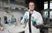
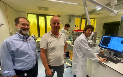
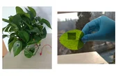
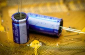
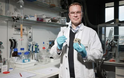
EPFL chemical engineers have invented a solar-powered artificial leaf, built on a novel electrode which is transparent and porous, capable of harvesting water from the air for conversion into hydrogen fuel. The semiconductor-based technology is scalable and easy to prepare.