Featured
What to know about the benefits of domestic prototyping
What to know about the benefits of domestic prototyping
PCB Trace Width Calculator
Glossary of Semiconductors Terms
What to know about the benefits of domestic prototyping
Find out what this complex piece of legislation means for electronics manufacturing.
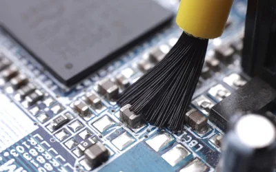
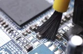
Learn the best methods and industry standards for cleaning circuit boards, removing contaminants like dust, flux residues, and corrosion to ensure optimal performance and longevity!
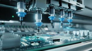
Semiconductors are the building blocks of modern electronics, powering everything from smartphones to satellites. This in-depth guide provides a comprehensive understanding of semiconductors' engineering principles and applications, delving into their fundamental concepts, materials, devices, manufacturing processes, and their impact on today's technology landscape.
13 minutes read.
20 minutes read.
16 minutes read.
20 minutes read.
20 minutes read.
13 minutes read.


Semiconductors
Nordic Semiconductor is a fabless semiconductor company specializing in wireless technology that powers the IoT.
181 Posts
A guide covering the full radio-frequency design workflow, starting from setting specifications and choosing topologies to matching, simulation, layout, and verification, to help antenna engineers.
This article presents a detailed technical exploration of SiC MOSFET devices, covering material physics, device structure, switching behavior, and practical design considerations for high-efficiency power electronics systems.
This article is a comprehensive technical guide to relay wiring diagrams, covering 4-pin and 5-pin configurations, working principles, safety practices, standards, and advanced relay applications in modern systems.
Explore how frequency shapes EMC behavior from RF emissions to ultra-low-frequency drift, with mitigation strategies for robust, compliant electronic system design.
How Essentra Components Supports Engineering from Concept to Production
Makera gives live demonstrations of the Z1 during the 2026 Hackaday Europe event. The Z1 is a compact CNC manufacturing platform.
A crystal oscillator is an electronic circuit that uses a quartz crystal to produce a precise and stable frequency reference. This article covers crystal operation, equivalent circuit models, resonance, load capacitance, oscillator topologies, stability, aging, and design practices.
June 25, 2026 at 08:00 PM Central European Summer Time
What to know about the benefits of domestic prototyping

4 minutes read
Find out what this complex piece of legislation means for electronics manufacturing.
Learn the best methods and industry standards for cleaning circuit boards, removing contaminants like dust, flux residues, and corrosion to ensure optimal performance and longevity!
Article #5 of the Enabling IoT Series. MEMS microphones can deliver high-quality sound in an ultra-small form-factor.
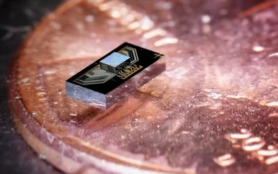
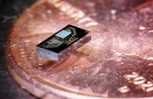
Engineers at Caltech and the University of Southampton have collaboratively designed an electronics chip integrated with a photonics chip (which uses light to transfer data)—creating a cohesive final product capable of transmitting information at ultrahigh speed while generating minimal heat.

3 minutes read
PCBs are extensively used across industries, powering devices from simple gadgets to complex systems. In this article, we’ll understand the importance of PCB thickness, the various factors affecting it, and its impact on design and other factors.
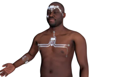
In this episode, we talk about the tattoo-like flexible wearable technology that’ll provide seamless high precision health monitoring for patients and enthusiasts.

Announcing TechBlick's free-to-attend virtual conference and exhibition covering innovations in Wearable Sensors | E-Textiles | Printed Electronics & Beyond. It is a unique event with two-parallel live tracks, a live engaging exhibition floor, and 400+ attendees. See details & registration link here

2 minutes read
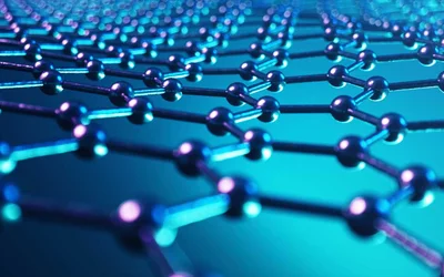
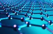
For the first time, ETH Zurich researchers have been able to make a superconducting component from graphene that is quantum coherent and sensitive to magnetic fields. This step opens up interesting prospects for fundamental research.

3 minutes read
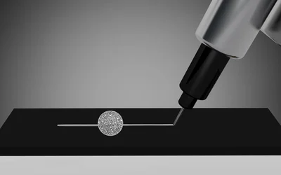
A unique new approach of printing functional materials with unparallel precision and repeatability. Technology called Ultra-Precise Deposition (UPD) is a nanodispensing method capable to print high density and high viscous materials with the resolution down to 1 µm in feature size and with high ratio of width to height after single pass. For this method material extrusion is controlled by a pressure, which means it is not supported with high electric field. Thanks to this there are no limitation if the substrate is conductive or dielectric.
2 minutes read
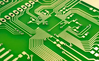
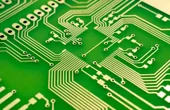
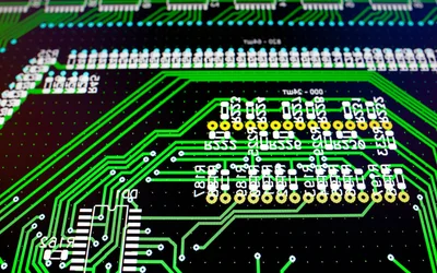
PCB traces are fundamental components in circuit design, serving as the pathways for electrical signals. This article examines the advancements, applications, and challenges of PCB trace technology. Discover insights into optimizing designs and overcoming common obstacles in PCB trace implementation.
With some foresight, most CAD design layout packages can accommodate castellated edge designs.
3 minutes read
Bringing a product to market late has a real and negative impact on profits and brand reputation. In this blog, we go through the types of documentation your project requires and ways to streamline processes.
3 minutes read
This article delves into the core variations between PMOS and NMOS, exploring their fundamentals, structural differences, operating principles, and practical applications.
Article #4 of the "Why Edge?" Series. A short guide to how Edge AI is enabling cutting-edge advances in the automotive industry.