Gate Driver Design for Modern Power Electronics
Understanding gate-driver fundamentals, architectures, drive techniques for SiC MOSFETs and GaN HEMTs, protection features, key specifications, and selection guidance for modern power electronics.

20 Apr, 2026. 13 minutes read
Key Takeaways
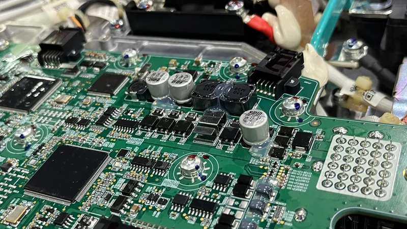
Gate drivers translate logic signals into high-current gate drive. They supply and remove charge from MOSFET, IGBT, and GaN transistor gates so that high-power switches operate quickly and efficiently.
Understanding gate charge and the Miller plateau is essential. The gate driver must deliver enough source and sink current to charge the gate capacitances through the Miller plateau. A high gate charge or long plateau increases switching losses.
Isolated drivers use optocoupler, capacitive, or magnetic coupling. They provide galvanic isolation and must meet standards such as UL 1577, IEC 60747-17, and VDE 0884-11. Key specifications include isolation voltage, common-mode transient immunity (CMTI), and propagation delay.
SiC and GaN devices impose unique drive requirements. SiC MOSFETs need +15 to +20 V gate drive and negative turn-off voltage to suppress dv/dt-induced turn-on. GaN HEMTs require low-voltage direct drive (0 V to 6 V) and meticulous control of dv/dt to prevent Miller turn-on.
Protection features are critical for reliability. Desaturation detection shuts down the gate when overcurrent increases collector-emitter voltage beyond ~7 V. Undervoltage lockout (UVLO), soft turn-off, and active Miller clamps prevent damage during faults and reduce false turn-on.
Selecting a gate driver involves balancing speed, isolation, and current. Engineers must consider propagation delay, CMTI, peak source/sink current, dead time, and isolation voltage relative to the target power device and application.
Introduction
Wide-bandgap semiconductors such as silicon carbide (SiC) and gallium nitride (GaN) are revolutionising power electronics. Compared with silicon, these materials support higher switching frequency, higher voltage, and lower conduction loss. They enable compact traction inverters, efficient motor drives, and high-density data-centre power supplies. However, the benefits of SiC and GaN come with gate drive challenges: devices must switch in tens of nanoseconds under hundreds of volts, survive high dv/dt and di/dt, and meet rigorous safety standards.
Gate driver circuits transform low-level control signals into the high-current pulses needed to charge and discharge transistor gates while providing isolation and protection. This article discusses gate-driver fundamentals, compares architectures, discusses drive techniques for SiC MOSFETs and GaN HEMTs, explains protection features, evaluates key specifications, and outlines application-oriented selection.
Gate Driver Fundamentals
Gate Charge and Miller Plateau
MOSFET, IGBT, and GaN devices are voltage-controlled, but the gate resembles a capacitor. Switching requires injecting or removing charge from three capacitances: gate-source capacitance Cgs, gate-drain (Miller) capacitance Cgd, and drain-source capacitance Cds. The total gate charge Qg is the integral of gate current over time and determines how much charge the driver must supply.
A critical region during switching is the Miller plateau. When a MOSFET turns on, the gate voltage rises quickly until it reaches the plateau, where the drain voltage begins to fall. During this plateau, the gate voltage stays nearly constant while the device's drain-source voltage slews. Charge is being transferred through the gate-drain capacitance, and the driver must supply current to complete this charge transfer.
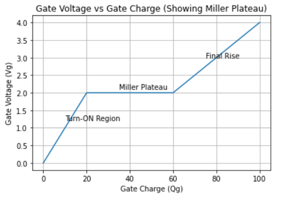
The plateau ends when the drain voltage settles, and the gate voltage then rises to the final value. Higher Qgd increases the plateau duration and switching losses. GaN devices have small Qgd but low threshold voltage, making them sensitive to dv/dt-induced turn-on.
Recommended Reading: How Do MOSFETs Work: Comprehensive Technical Guide for Engineers (2025)
Source and Sink Current
Gate drivers must both source and sink current. Sourcing current charges the gate capacitance to turn the switch on; sinking current discharges it for turn-off. The peak current capability sets how fast charge can be moved.
A large source current speeds up turn-on but may cause ringing and electromagnetic interference (EMI).
A large sink current is vital for fast and clean turn-off, especially with wide-bandgap devices.
Gate driver ICs specify peak source/sink currents, often asymmetrical. For example, the Texas Instruments UCC21520 provides 4 A source and 6 A sink current with a typical propagation delay of 33 ns and CMTI >125 V/ns.
Dead Time and Control Signals
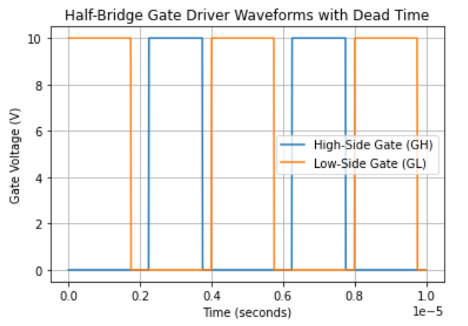
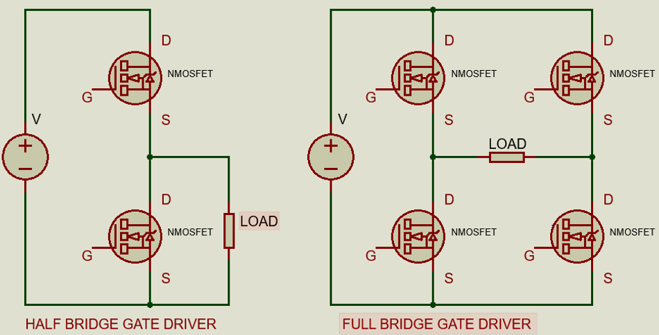
In half-bridge or full-bridge topologies, one transistor must turn off completely before the complementary device turns on. Dead time is inserted between switching transitions to avoid shoot-through.
If the dead time is too short, it causes cross-conduction and high losses. Likewise, if it’s too long, it increases conduction losses in freewheeling diodes. Gate driver ICs may include built-in programmable dead-time control.
Propagation Delay and Timing Skew
Propagation delay is the time between the driver input and output transitions. In high-frequency converters, small mismatches in propagation delay between phases can reduce efficiency or distort current sharing.
Leading gate driver ICs deliver delays under 50 ns; for instance, the UCC21520's typical delay is 33 ns, while Infineon's 1ED3124 has ~90 ns.
Non-Isolated Gate Drivers
Non-isolated gate drivers connect directly to the control ground. They are used in synchronous buck converters, DC-DC modules, and motor drives where isolation is not mandatory.
Bootstrap High-Side Drive
In half-bridge circuits, the high-side gate voltage must exceed the supply voltage to turn on the transistor. A bootstrap circuit uses a diode and a capacitor to create a floating supply referenced to the switching node. When the low-side transistor is on, the bootstrap capacitor charges.
When the high-side device turns on, the capacitor's voltage adds to the supply to drive the gate. This simple and cost-effective approach suits high-frequency DC-DC converters. However, the capacitor must be refreshed each cycle, limiting the duty cycle to below 100%. Also, the bootstrap diode must withstand high dv/dt.
Charge Pump Drivers
A charge pump uses switched capacitors to generate a steady floating supply for the high-side driver. It is free from duty-cycle constraints and provides continuous supply. Charge-pump drivers are common in gate driver ICs for high-side MOSFETs operating at high duty cycles or full-bridge topologies.
Half-Bridge Drivers
Half-bridge gate driver ICs integrate both low-side and high-side drivers with built-in dead-time control, UVLO, and level shifting. For instance, TI's UCC27211 offers 120 V bootstrapped high-side drive with 4 A peak current, while onsemi's NCP51530 provides 600 V half-bridge drive. These non-isolated drivers power synchronous buck converters, motor drives, and point-of-load supplies.
Suggested Reading: Buck Converters: A Comprehensive Guide for Hardware Design Engineers
Isolated Gate Drivers
High-voltage converters, automotive traction inverters, and server power supplies require galvanic isolation between the control circuitry and power stages. Isolation protects low-voltage logic from large common-mode transients and ensures safety compliance.
Isolation Technologies
Optocoupler Gate Drivers
Optocouplers use an LED and a photodiode to transfer signals across an insulation barrier. Broadcom's ACPL-332J is an isolated gate driver optocoupler. It features a 2.5 A (min 2.0 A) peak output current, a typical propagation delay of 250 ns, an integrated Miller clamp (1.7 A), and UVLO.
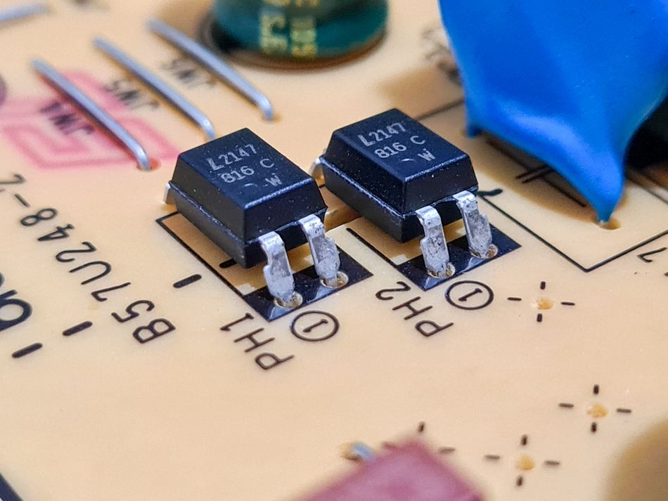
The device withstands 5 kVrms isolation for one minute and meets UL 1577 certification. Optocouplers are robust but have longer propagation delay and ageing issues due to LED efficiency decline.
Capacitive Digital Isolators
Capacitive isolators transmit digital signals across a silicon dioxide barrier using differential capacitors. Silicon Labs Si827x family provides 5 kVrms insulation, with a propagation delay around 60 ns and a CMTI over 200 kV/us.
They feature separate outputs for pull-up and pull-down to optimise source and sink currents, and meet UL 1577 and VDE 0884-11 standards.
Magnetic Isolators and Coreless Transformers
Magnetic isolators use inductive coupling on a silicon substrate. Analog Devices' ADuM4135 employs a transformer-based isolation scheme, delivering a short-circuit source current of 13 A and sink current of 14 A with a peak of 4.61 A and propagation delay of about 55 ns.
Its CMTI exceeds 100 kV/us and isolation voltage is rated 5 kV ac with compliance to DIN VDE V 0884-11. Magnetic isolators achieve high speed and robustness.
Coreless Transformer Drivers
Infineon's EiceDRIVER 1ED31xx family uses a silicon transformer for isolation. The 1ED3124, for example, delivers 14 A typical source and sink current, propagation delay around 90 ns, and CMTI >200 kV/us. It provides reinforced isolation of 5.7 kVrms per UL 1577 and meets IEC 60747-17 guidelines. Coreless transformers offer excellent CMTI and integration.
Suggested Reading: Electrical Transformers: Engineering Fundamentals, Design Parameters, and Emerging Trends
Common-Mode Transient Immunity (CMTI)
CMTI is the maximum rate of change of common-mode voltage that an isolator can withstand without erroneous switching. In SiC and GaN converters, dv/dt can exceed hundreds of kilovolts per microsecond.
High CMTI prevents false triggering or communication errors. Gate driver ICs with CMTI ratings above 100 kV/us ensure reliable drive under fast transients.
Isolation Standards
Isolated gate drivers must comply with safety standards. UL 1577 defines isolation test methods and is widely used for consumer and industrial equipment. IEC 60747-17 covers reinforced isolation for semiconductor devices, specifying creepage distances and surge isolation.
VDE 0884-11 sets requirements for digital isolators, including partial discharge and lifetime testing. When selecting a driver, confirm certification and isolation rating; for example, UCC21520 offers 5.7 kVrms per UL 1577 and 8000 Vpk per IEC 60747-17.
Suggested Reading: Whats The Difference Between UL And IEC Standards?
Gate Driving SiC MOSFETs
SiC MOSFETs switch at high voltage and frequency, requiring robust gate drive to harness their speed and avoid false turn-on.
Gate Voltage and Negative Bias
SiC MOSFETs typically require gate voltages of +15 V to +20 V for full enhancement and a negative voltage at turn-off to improve dv/dt immunity. A +20 V gate drive and a negative off voltage between -2 V and -6 V improve switching behavior and minimize false triggering.
Negative bias helps hold the gate firmly off and offsets the Miller effect, especially at high dv/dt. Many drivers include a negative supply or charge pump to generate the negative rail; for example, onsemi's NCP51705 integrates an adjustable negative charge pump and supplies 6 A source and sink current.
Suggested Reading: N-Channel MOSFET Basics: Theory, Operation and Practical Implementations
Kelvin Source Connection
To reduce voltage overshoot and ringing, SiC MOSFETs often provide a separate Kelvin source pin for the gate driver return. Connecting the driver's return directly to the Kelvin source isolates the gate loop from large source inductances that arise in power traces.
This minimises voltage spikes and ensures accurate gate voltage. Gate driver PCBs should place gate and return traces close together and avoid loops.
Desaturation Detection and Short-Circuit Response
SiC MOSFETs can fail catastrophically under short circuits. Desaturation (DESAT) detection monitors the drain-source voltage; when an overcurrent increases this voltage beyond ~7 to 9 V, the driver turns the gate off quickly to protect the device. Some drivers implement soft turn-off, controlling gate discharge to limit di/dt and voltage overshoot
Active Miller Clamp
During turn-off, the drain voltage rises, coupling through Cgd and raising the gate voltage. An active Miller clamp holds the gate close to ground (or negative bias) by shorting it to the source when the gate voltage falls below a threshold.
This prevents the gate from being pulled above the turn-on threshold by dv/dt. Many SiC-capable drivers integrate a Miller clamp; the ACPL-332J provides a 1.7 A Miller clamp current, while the ADuM4135 integrates a clamp and desaturation detection.
Suggested Reading: Silicon Carbide (SiC) Wafers: Revolutionizing Power Electronics and Beyond
Gate Driving GaN HEMTs
GaN HEMTs deliver extremely fast switching with low on-resistance and no reverse recovery charge, but they require careful gate drive due to low threshold voltage and limited gate-source voltage.
Low Drive Voltage and Threshold
GaN devices operate with gate-source voltages typically from 0 V to 6 V. The maximum gate-source voltage is +/-6 V, and the threshold voltage is only 0.7 V to 2.5 V. Overvoltage can destroy the gate, while even small dv/dt may cause unintended turn-on. Therefore, drivers must regulate the gate voltage precisely and avoid overshoot.
Direct Drive and Low Gate Resistance
Because GaN devices have no body diode and small gate charge, they can be driven directly by logic-level drivers, but the driver must control current and dv/dt. To prevent the drain-gate capacitance from pulling up the gate during dv/dt, the gate resistance should be low.
Reducing resistance increases dv/dt immunity. Many GaN-specific driver ICs include low impedance outputs and adjustable gate resistance.
Fast Transitions and Layout Considerations
GaN HEMTs switch in a few nanoseconds, so parasitic inductance must be minimised. Gate drive loops should be very short, with ground planes and Kelvin connections. Layout guidelines include using coplanar or embedded traces and avoiding stubs. Drivers like onsemi's NCP51705 provide 6 A peak current and propagation delays of 25 to 50 ns, enabling rapid transitions.
Suggested Reading: Where GaN can, it should, and GaN can in more and more places
Gate Driver Protection Features
Desaturation Detection
Desaturation detection monitors the drain or collector voltage and detects short-circuit currents. When the drain-source voltage rises above a threshold (often ~7 V to 9 V for IGBTs and SiC MOSFETs), the driver triggers a fault response. It often incorporates blanking time and noise filters to avoid spurious trips. After detection, the driver typically initiates a controlled soft turn-off to limit di/dt and protect the device.
Undervoltage Lockout (UVLO)
UVLO ensures that the driver only switches the gate when the supply voltage is within safe limits. If the supply is below a threshold, the driver holds the gate low, preventing partial turn-on that could lead to high dissipation. Many drivers have separate UVLO thresholds for the high-side and low-side or for the positive and negative rails.
Soft Turn-Off and Two-Stage Turn-Off
During fault conditions, abruptly turning off a device can create a large overvoltage due to stray inductance. Soft turn-off uses a two-stage discharge: initially a moderate current to slow the turn-off, then a stronger current once the drain voltage has risen. This reduces di/dt and overvoltage stress. Some drivers provide adjustable soft turn-off timing.
Key Specifications
Comparison of Representative Gate Driver ICs
Driver IC | Vendor | Isolation Type | Isolation Voltage | Propagation Delay (typ) | Peak Source/Sink Current | CMTI | Key Features |
UCC21520 | Texas Instruments | Coreless transformer | 5.7 kVrms (UL 1577) | ~33 ns | 4 A / 6 A | >125 kV/us | Dual-channel, 8000 Vpk per IEC 60747-17 |
1ED3124 | Infineon | Coreless transformer | 5.7 kVrms (UL 1577) | ~90 ns | 14 A / 14 A | >200 kV/us | Separate source/sink outputs, short-circuit clamping |
NCP51705 | onsemi | Non-isolated | N/A | 25-50 ns | 6 A / 6 A | High | Adjustable negative charge pump, DESAT, thermal shutdown |
Si8271 | Silicon Labs | Capacitive | 5 kVrms | ~60 ns | 4 A / 4 A | >200 kV/us | UL 1577 and VDE 0884-11 compliance |
ACPL-332J | Broadcom | Optocoupler | 5 kVrms | ~250 ns | 2.5 A peak | 50 kV/us | Integrated Miller clamp, DESAT, UVLO |
ADuM4135 | Analog Devices | Magnetic | 5 kV ac (UL 1577) | ~55 ns | 13 A / 14 A (SC) | >100 kV/us | Integrated Miller clamp, DESAT, VDE 0884-11 |
Applications of Gate Drivers and Selection Criteria
Electric-Vehicle (EV) Inverters
Traction inverters drive three-phase motors using SiC MOSFETs or IGBTs. The driver must handle bus voltages up to 800 V, supply currents of 600 to 1000 A, and switching frequencies around 10 to 20 kHz
Reinforced isolation is mandatory, along with high CMTI and robust protection. Dual-channel isolated drivers like TI's UCC21520 or Infineon's 1ED31xx provide symmetric drive for high-side and low-side devices, while offering 5 kVrms isolation and CMTI beyond 100 kV/us.
Solar Inverters and Power Factor Correction (PFC)
Residential and commercial solar inverters use half-bridge and full-bridge topologies at 600 to 1500 V. They often employ SiC MOSFETs to reduce switching losses. Gate drivers must deliver high efficiency at tens of kilohertz and include soft shutdown. Isolation is essential for grid safety.
Motor Drives and Servo Systems
Industrial motor drives operate across a wide range of power levels. Low-power drives use MOSFETs, while high-power drives use IGBTs or SiC devices. Gate drivers must provide high current and support field weakening, free-wheeling, and regeneration. The Broadcom ACPL-332J optocoupler driver offers integrated DESAT detection and a Miller clamp for IGBT modules.
Suggested Reading: Powering Electric Motor Drives
Server Power Supplies and Data-Centre Converters
Data centres demand high-efficiency power conversion at 400 to 48 V and high current. GaN FETs are increasingly used in AC-DC front ends and DC-DC converters.
Gate drivers must deliver fast switching at frequencies up to several megahertz and regulate low gate voltage precisely. Non-isolated half-bridge drivers with high peak current such as onsemi's NCP51705, meet this need.
Selection Guidelines for Gate Drivers
Here is a quick look at basic selection guidelines for picking a suitable gate driver:
Identify the power device (MOSFET, IGBT, SiC MOSFET, or GaN HEMT). Each has different gate voltage range and required current.
Determine isolation needs. For high-voltage or safety-critical systems, choose an isolated driver with appropriate voltage and certification.
Evaluate switching frequency and dv/dt. Higher frequency demands lower propagation delay and high CMTI.
Calculate required gate charge and drive current. Use the device datasheet to compute peak source and sink current. Add margins for driver losses and EMI control.
Check protection features. DESAT detection, UVLO, soft turn-off, Miller clamp, and thermal shutdown are vital for reliability.
Review package and thermal considerations. Large gate currents may necessitate packages with low thermal resistance or separate outputs for source and sink.
Conclusion
The gate driver sits at the nexus of power devices and control logic, translating digital commands into the current pulses that charge and discharge transistor gates. As power electronics push towards higher frequency, higher voltage, and greater efficiency, gate drivers must deliver larger currents, withstand extreme common-mode transients, and incorporate advanced protection.
Engineers have a broad choice of ICs from major vendors, offering coreless transformer, capacitive, magnetic, and optocoupler isolation with varying current capabilities and protection features. Looking ahead, integration of gate drivers into power modules, co-packaging with GaN and SiC switches, and digital programmability will continue to enhance system performance and simplify design.
FAQ
1. Why is the Miller plateau significant when sizing a gate driver?
During the Miller plateau, the drain voltage is falling while the gate voltage remains nearly constant. The gate driver must supply sufficient current to charge the gate-drain capacitance and overcome the plateau. A high Miller charge slows switching and increases losses. Selecting a driver with adequate source current and optimising gate resistance ensures that the plateau is traversed quickly without excessive ringing.
2. What is CMTI and how does it affect operation?
CMTI is the maximum rate of change of the voltage across the isolation barrier that a driver can tolerate without producing spurious output. Fast dv/dt transients in SiC and GaN converters can induce errors if CMTI is insufficient. High-CMTI drivers maintain correct operation even when the switching node voltage changes by tens or hundreds of kilovolts per microsecond.
3. Why do SiC MOSFETs require negative gate bias?
SiC MOSFETs have higher threshold voltages and strong reverse transfer capacitances. At high dv/dt, the Miller effect can raise the gate voltage above the threshold even when the gate is tied to ground. Applying a negative bias during turn-off (typically -2 V to -5 V) ensures the gate remains firmly off and enhances dv/dt immunity. Negative bias also reduces switching losses by discharging the gate more completely.
4. What challenges arise when driving GaN HEMTs?
GaN HEMTs have low gate threshold voltage and limited gate-source voltage. They operate from 0 V to ~6 V and can be damaged by overvoltage. Their small gate charge and fast switching make them sensitive to dv/dt-induced turn-on. Drivers must deliver clean, regulated gate voltage with minimal overshoot and include low impedance pull-down paths.
5. How does desaturation detection protect power devices?
Desaturation detection monitors the drain-source or collector-emitter voltage. Under short-circuit conditions, the device cannot sustain the current and its voltage rises rapidly. When the voltage exceeds ~7 to 9 V, the driver's DESAT circuit triggers and shuts off the gate. This prevents catastrophic failure. The protection often includes blanking to avoid false trips and soft turn-off to limit overvoltage.
6. What are the primary standards governing isolated gate drivers?
UL 1577 specifies isolation test methods for semiconductor isolators. IEC 60747-17 defines reinforced isolation for semiconductor devices, including creepage and surge requirements. VDE 0884-11 addresses digital isolators and defines partial discharge and lifetime testing.
References
Texas Instruments. UCC21520 Isolated Dual-Channel Gate Driver datasheet.
https://www.ti.com/lit/ds/symlink/ucc21520.pdfInfineon. EiceDRIVER 1ED31xx technical documentation.
https://www.infineon.com/assets/row/public/documents/24/49/infineon-1ed312xmu12f-datasheet-en.pdfonsemi. NCP51705 gate driver datasheet.
https://www.onsemi.com/download/data-sheet/pdf/ncp51705-d.pdfSilicon Labs. Si827x Digital Isolator Gate Driver datasheet.
https://www.skyworksinc.com/-/media/Skyworks/SL/documents/public/data-sheets/Si827x.pdfBroadcom. ACPL-332J optocoupler gate driver datasheet.
https://datasheet4u.com/datasheets/AVAGO/ACPL-332J/742951Analog Devices. ADuM4135 isolator gate driver datasheet.
https://www.analog.com/en/products/adum4135.htmlInfineon Developer Community. Common-Mode Transient Immunity article.
PowerElectronicTips. What is Gate Charge and Why Does It Matter?
https://www.powerelectronictips.com/what-is-gate-charge-and-why-does-it-matter-for-switching-speed/EPC. eGaN FET Drivers: Maximising Performance white paper.
How2AppNote005 Growing GaN Ecosystem.pdfonsemi. Driving SiC MOSFETs application note.
EVBUM2731.rev1DIN VDE V 0884-11:2017-01 Standard.
What the DIN VDE V 0884-11:2017-01 standard means for your isolated designs
in this article
1. Key Takeaways2. Introduction3. Gate Driver Fundamentals4. Non-Isolated Gate Drivers5. Isolated Gate Drivers6. Gate Driving SiC MOSFETs7. Gate Driving GaN HEMTs8. Gate Driver Protection Features9. Key Specifications10. Applications of Gate Drivers and Selection Criteria11. Conclusion12. FAQ13. References