What is Co-Packaged Optics: Architecture, Benefits, Challenges, and Performance
Co-packaged optics integrates photonic engines directly with switch ASICs and AI accelerators, cutting power draw and latency at the board level. This article explains how CPO works, how it compares to pluggable and near-packaged optics, and what its benefits and challenges are.

24 Apr, 2026. 19 minutes read
Key Takeaways
Co-packaged optics (CPO) integrates optical engines directly adjacent to the switch ASIC or accelerator, shortening electrical traces and eliminating the need for DSP retimers. This proximity reduces power consumption dramatically. Experiments show that a 30 W pluggable transceiver can be replaced by a 9 W CPO link, a 70% power reduction.
Collapsing electrical distances to millimeter scales pushes energy efficiency toward sub-picojoule-per-bit targets. Silicon photonics tiles with 3D packaging deliver up to 6.4 Tb/s per tile and form 51.2 Tb/s to 102.4 Tb/s switches at bandwidth densities that pluggables cannot match [2][10].
Removing long copper paths improves signal integrity and reduces latency by eliminating the overhead of equalization and retiming. This shrinks link budgets and allows SerDes lanes at 200 Gbit/s to drive optical engines directly [3].
CPO introduces real engineering tradeoffs: thermal management is harder when photonics sit next to hot logic, fiber attach at scale is complex, and co-locating optics with the ASIC complicates yield, test, and field serviceability. High-density fiber harnesses add further integration challenges [4].
Broadcom's Tomahawk 6 and related next-gen CPO switch ASICs are targeted for commercial availability in the 2025–2026 window [10]. Broad adoption of CPO in scale-up GPU interconnects — where the power and density gains matter most — is expected between 2028 and 2030 as supply chains and standards mature. [7].
The industry is converging on modular optical engines (1.6T–6.4T), external laser sources, and standardized fiber connectors. Broadcom, Marvell, Ayar Labs, and Ciena are pursuing distinct architectural approaches, giving engineers choices across bandwidth density, power efficiency, serviceability, and cost.
Introduction
The growth of artificial intelligence (AI) models and high-performance computing (HPC) is imposing unprecedented demands on data-center interconnects. Traditional copper backplanes and pluggable optical transceivers are hitting power and bandwidth limits. Modern switches already support 51.2 Tb/s, and roadmaps call for 100 Tb/s and beyond [2]. Each GPU often requires multiple 30 W pluggable transceivers. Scaling to tens of thousands of GPUs would consume hundreds of megawatts [8]. In parallel, as port counts and data rates climb, copper traces struggle to maintain signal integrity over board-level distances, leading to insertion losses that demand costly equalization and retimers. Engineers need interconnects that deliver higher bandwidth per watt, lower latency, and better scalability.

Co-packaged optics (CPO) addresses this bottleneck by integrating optical engines next to switch ASICs or accelerators within the same package. By converting electrical signals to light within a few millimeters of the silicon, CPO shortens copper paths, eliminates high-power DSPs, and allows the photonic engine to drive optical fibers directly. Early deployments, such as Broadcom's Bailly CPO switch ASIC and NVIDIA's Quantum-X Photonics — which targets scale-up InfiniBand interconnects — have demonstrated dramatic power savings and bandwidth density.
This article explains the theory behind co-packaged optics, examines practical implementations, and compares them with pluggable optics and the emerging near-packaged optics (NPO) paradigm. It also analyzes the challenges and trade-offs engineers must consider when designing CPO systems, and surveys the vendor landscape and roadmap for AI data centers.
What is Co-Packaged Optics?
Co-packaged optics refers to the integration of optical transceivers and photonic components directly adjacent to an electronic integrated circuit (switch ASIC or AI accelerator) on the same substrate or within the same package. Unlike pluggable optics, where optical modules sit on the front panel and connect to the switch via long PCB traces and cages, CPO brings the photonic engine within millimeters of the ASIC. The shorter electrical path means less signal loss, lower power draw, and higher data rates. The integration can be 2.5D (on a silicon interposer) or 3D (using die stacking approaches such as chip-on-wafer or die-to-die bonding), with interconnect methods varying by implementation, including through-silicon vias, hybrid bonding, or combinations of both.
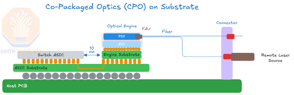
By placing the optical engine near the electrical source, CPO minimizes electrical path length, improving signal integrity and reducing power consumption [7]. This architecture also allows higher SerDes rates (200 Gbit/s or more) without DSP retimers [3], enabling bandwidth densities that exceed what can be delivered through front-panel pluggables. CPO is distinct from near-packaged optics (NPO), which places photonic engines at the edge of the PCB close to the ASIC but still outside the package. NPO reduces path length relative to pluggables but does not fully integrate the optics.
Recommended Reading: What is an ASIC: A Comprehensive Guide to Understanding Application-Specific Integrated Circuits
Components of a CPO Package
Co-packaged solutions combine several building blocks:
Switch ASIC or Accelerator: A high-radix, high-bandwidth silicon device that routes or processes data. Broadcom's Tomahawk 6 targets 102.4 Tb/s with CPO integration [10]; NVIDIA's Quantum-X targets 51.2 Tb/s in InfiniBand scale-up networks [2]. These serve distinct network domains, but both represent the leading edge of ASIC bandwidth. [2][10].
Photonic Integrated Circuit (PIC): A silicon photonics die containing waveguides, modulators, drivers, and photodetectors. Modulation technology varies: Mach-Zehnder modulators (MZM) in early CPO, micro-ring modulators (MRM) in NVIDIA's second-generation implementation, which contributed to significant system-level power reductions [1], and electro-absorption modulators (EAM) under evaluation for upcoming 400G lanes.
Electronic IC (EIC): A CMOS die that houses SerDes, drivers, control logic, and power management. It interfaces with the ASIC through high-speed electrical channels and controls the PIC.
Optical Engine / Light Engine: A module combining the PIC and EIC with fiber array units. Engines deliver aggregate bandwidths of 1.6 T to 6.4 T per tile. Broadcom's Bailly CPO uses eight 6.4 Tb/s silicon-photonic engines surrounding the ASIC [5]. NVIDIA's quantum design uses 1.6 Tb/s engines built with TSMC's COUPE process and groups three engines into 4.8 Tb/s optical sub-assemblies (OSAs) that can be detached for serviceability [2].
External Light Source (ELS): To improve reliability and thermal management, lasers are often moved off the ASIC package. Laser modules feed light into the PIC via waveguides. Vendors such as Ayar Labs use the SuperNova 16-wavelength laser for their TeraPHY chiplets [8]. Moving the laser externally simplifies cooling and allows redundancy.
Fiber Attach & Connectors: Dense fiber arrays bring optical signals from the engines to the rack. CPO uses edge coupling (as in Broadcom's epoxy-bonded fibers) or surface coupling (as in NVIDIA's microlens approach). Advanced connectors such as Corning's GlassBridge and CPO FlexConnect provide detachable fiber harnesses and support thousands of fibers [5]. Marvell's reference design reportedly uses 32 metallic PIC couplers per compute tray, with fiber counts in the tens of thousands [4].
How Co-Packaged Optics Works
Data moves through a CPO system in four stages that happen in rapid succession. First, the switch ASIC or accelerator sends high-speed electrical signals to the electronic IC (EIC) through on-package interconnects. Because these copper traces are only millimeters long, SerDes lanes can run at up to 100 Gb/s per lane in current implementations — with 200 Gb/s targeted in next-generation designs — without the heavy equalization that longer PCB traces demand [3].
The EIC then drives modulators on the photonic IC (PIC), which encodes the electrical data onto light for high-speed data transfer. Depending on the design, this is done using Mach-Zehnder modulators (MZMs), micro-ring modulators (MRMs), or electro-absorption modulators (EAMs). MRMs are particularly attractive because they are physically smaller and require lower drive voltages, which translates directly to lower energy per bit. On the receive side, photodetectors on the same PIC convert incoming optical signals back to electrical ones.
Once encoded, light travels through on-chip waveguides to a fiber array unit at the edge of the package. Grating couplers or expanded-beam couplers bridge the gap between the waveguide and the optical fiber, with grating couplers typically tolerating alignment offsets on the order of ±20 µm [6]. Detachable connectors such as Corning's GlassBridge and Marvell's metallic PIC couplers allow the fiber harness to be disconnected from the package without disturbing the ASIC, which matters for field serviceability.
Light itself comes from an external laser source (ELS) sitting outside the ASIC package — often mounted in the switch chassis or front panel. The ELS generates continuous-wave light at one or more wavelengths and distributes it to multiple optical engines via optical splitters or wavelength multiplexers. Keeping the laser external reduces heat on the ASIC package and improves overall system reliability.
Comparison with Pluggable and Near-Packaged Optics
Pluggable optics remain the dominant form factor for network switches due to their standardization and ease of maintenance. However, they rely on long PCB traces and high-power DSP retimers. A 1.6 Tb/s pluggable module typically consumes around 25 W [6].
NPO is related to but distinct from linear pluggable optics (LPO), which removes the DSP from the module itself without necessarily relocating the optics. The table below contrasts these approaches.
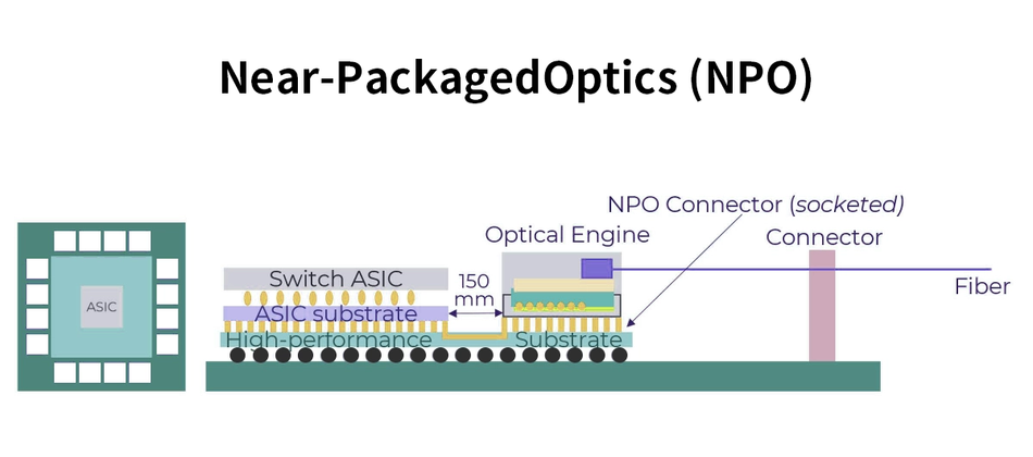
Metric / Feature | Pluggable Optics | Near-Packaged Optics (NPO) | Co-Packaged Optics (CPO) |
Electrical path length | ~15-30 cm from ASIC to module; requires high-loss LR SerDes and DSP retimers [1] | ~2-5 cm; reduced loss but still needs some equalization | Millimeters; eliminates DSPs and retimers [3] |
Power per bit | 15–20 pJ/bit; fully retimed 1.6T module, typically 20–22 W | 8-15 pJ/bit; improved by shorter traces | 5–10 pJ/bit demonstrated; sub-5 pJ/bit in early implementations; example 1.6 T CPO link ≈5 W [6] |
Bandwidth density | Limited by front-panel cage area and fiber count | Moderate; still restricted by board routing | Highest; 6.4 T engines allow >51 Tb/s per switch with multiple engines [5] |
Serviceability | Excellent; modules are hot-swappable | Moderate; modules near ASIC but accessible | Varies; some platforms use detachable OSAs (NVIDIA) while others permanently bond engines (Broadcom). Requires careful packaging [2] |
Thermal management | Module power dissipates near the front panel; easier cooling | Closer to ASIC; shared thermal solution | Photonics, next to ASIC, requires advanced cooling; often liquid cooled [4] |
Deployment timeline | Mature; widely deployed across Ethernet generations | Emerging; used for linear pluggable optics (LPO) | Early deployment (2025-26) for scale-out; scale-up adoption expected 2028-30 [7] |
Architecture and Implementation
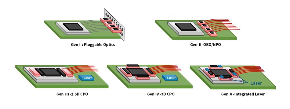
CPO is not a single architecture but a family of design approaches, and the differences between implementations reflect real engineering tradeoffs rather than arbitrary vendor choices. Understanding those tradeoffs — in integration topology, laser placement, and fiber attach — explains why no two CPO switches look quite the same.
Integration Topology: 2.5D vs 3D
The central packaging question in CPO is how tightly to couple the electronic IC (EIC) and photonic IC (PIC). In 2.5D integration, both dies sit side by side on a passive silicon interposer connected through microbumps or copper pillars. This reduces parasitic inductance compared to conventional PCB routing and supports high I/O density, but the signal still crosses two bump interfaces between the ASIC and the optical engine, which adds parasitics and limits how aggressively the electrical path can be shortened.
3D hybrid integration goes further by stacking the EIC directly on top of the PIC, achieving higher performance through minimized packaging parasitics, though at greater thermal and manufacturing complexity. MapYourTech TSMC's COUPE process used in NVIDIA's optical engines is an example of 3D stacking.
2.5D offers high-density interconnects and relative simplicity but faces scalability and thermal challenges; 3D reduces footprint and power consumption but increases process complexity. Santec's first-generation CPO switches use 2.5D integration for the system-level package — placing optical engines around the ASIC on an organic substrate — while using 3D stacking within the optical engine itself.
Laser Architecture: External vs On-Package
Early CPO designs placed lasers on the PIC, which simplified the optical path but created two problems: lasers are the least reliable component in the assembly, and they generate heat directly adjacent to temperature-sensitive modulators and the ASIC. The industry has converged on external laser sources (ELS) as the preferred solution.
By routing continuous-wave light from a laser module mounted on the switch chassis or front panel into the optical engines via fiber, designers keep laser heat away from the ASIC package and allow lasers to be replaced independently without touching the switch. Ayar Labs' SuperNova, for example, supplies 16 wavelengths to their TeraPHY chiplets from a separate, field-replaceable module. The tradeoff is insertion loss in the fiber path from laser to engine, which must be kept within the optical power budget of the PIC's modulators.
Fiber Attach: Fixed vs Detachable
How optical fibers connect to the package is one of the most consequential mechanical decisions in CPO design, and it has a direct impact on serviceability. Edge coupling — where fibers are aligned to waveguide facets at the chip edge and bonded with epoxy — is the most established approach and offers low insertion loss, but the bond is permanent. Surface coupling uses grating couplers or microlenses on the top surface of the PIC to redirect light vertically into fiber arrays, which permits looser alignment tolerances and enables detachable connectors.
Corning's GlassBridge uses glass waveguide connectors for high-density, detachable fiber attachment, while Marvell's metallic PIC couplers offer another detachable option. The core tradeoff is insertion loss versus serviceability: edge-coupled fixed harnesses perform better optically but make field replacement of fiber runs difficult; detachable surface-coupled connectors add loss but allow the fiber harness to be disconnected without disturbing the ASIC package.
Scale-Out vs Scale-Up Implementations
These architectural choices play out differently depending on whether the CPO system targets scale-out or scale-up networking. In scale-out — connecting thousands of switches in an Ethernet fabric — the priority is port density and cost per bit. Optical engines here are typically silicon-photonics based, running PAM4 at 200 Gb/s per lane, and the switch ASIC dominates the package design with multiple engines arranged around its perimeter. In scale-up — connecting GPUs within a compute node or rack — the requirements shift toward lower latency, higher bandwidth density per accelerator, and longer reach. This is where chiplet-based optical I/O, such as Ayar Labs' TeraPHY, becomes relevant: rather than surrounding a switch ASIC with optical engines, the optical interface is integrated directly into the accelerator package via standards like UCIe, enabling chip-to-chip optical links that bypass the switch entirely. These are architecturally distinct from switch-level CPO and serve a different point in the network hierarchy, though both fall under the CPO umbrella.
Key Technical Benefits
Bandwidth Density and Scalability
Pluggable optics are physically constrained by the front panel — there are only so many cages you can fit on a faceplate, and each one draws power and generates heat. CPO removes that ceiling. By wrapping optical engines directly around the switch ASIC, designers can pack far more bandwidth into the same footprint, and scale that bandwidth by adding engines rather than redesigning the board.
This makes CPO particularly attractive for the hyperscale switches that form the spine of AI training clusters, where bandwidth demand doubles every few years, and physical density is as important as raw throughput.
Power Efficiency
Power is the defining constraint of the modern data center, and optical interconnects are a significant contributor to the overall power budget. The inefficiency in pluggable architectures is structural — signals must be driven across centimeters of lossy PCB trace, recovered by a DSP, and retimed before reaching the optical engine. Each of those steps burns power. CPO eliminates most of that overhead by shortening the electrical path to millimeters and removing the DSP entirely. The result is a dramatic reduction in energy per bit, which at the scale of tens of thousands of GPUs translates directly into megawatts of saved capacity and lower cooling infrastructure costs.
Latency and Signal Integrity
Copper traces degrade signals. The longer the trace, the more equalization is needed, and equalization adds latency. DSP retimers compound this — they recover the signal but introduce additional processing delay. In synchronous AI workloads, where thousands of GPUs must coordinate gradient updates, latency determinism matters as much as raw speed. CPO addresses this at the source by keeping electrical paths short enough that signals reach the modulator cleanly, without retiming. The result is lower and more predictable latency, which improves the efficiency of distributed training at scale.
Reach and Topology Flexibility
Once data is on fiber, distance becomes cheap. Copper interconnects inside a rack are limited to a meter or two before signal integrity becomes a problem at high lane rates. Optical links from a CPO switch can reach across a row, across a room, or between buildings without repeaters. This gives network architects more freedom in how they lay out compute clusters — GPU pods no longer need to be physically adjacent to the switches serving them, and topologies like fat trees and dragonfly networks become easier to build with fewer switching stages. As AI clusters grow toward a million-GPU scale, that flexibility in physical layout becomes a meaningful operational advantage.
Challenges and Trade-Offs
Thermal Management and Cooling
Silicon photonics components are temperature-sensitive in a way that purely electronic systems are not. Wavelength drift in modulators and lasers can degrade optical performance with even modest temperature swings, and placing photonic engines directly adjacent to a high-power switch ASIC creates exactly the kind of concentrated heat that is difficult to manage. Traditional air cooling is increasingly inadequate at the power densities CPO switches operate at, pushing designers toward liquid cooling solutions such as cold plates. This adds system-level complexity and cost, and requires careful thermal modeling to ensure that transient hot spots — during traffic bursts, for example — do not push components outside their operating range.
Fiber Management and Serviceability
Every optical engine in a CPO switch requires fiber connections, and a fully populated switch can involve hundreds to thousands of individual fiber paths. Managing that density at the chassis level — routing, bending radius, connector access — is a non-trivial mechanical engineering problem. It is made harder by the serviceability constraints of co-packaged designs. Where a pluggable module can be swapped in seconds, a CPO optical engine with a permanently bonded fiber attachment requires significantly more intervention to replace.
Some vendors address this with detachable fiber connectors or modular optical sub-assemblies that can be removed without disturbing the ASIC, but these approaches introduce their own insertion loss penalties. Serviceability remains one of the strongest arguments operators make for staying with pluggables.
Manufacturing and Yield
CPO requires heterogeneous integration of semiconductor materials and processes that don't naturally belong together — CMOS electronics, silicon photonics, and in some designs, III-V laser materials. Each integration step is a potential yield loss point, and because rework is limited once components are bonded, a defect at any stage can write off the entire assembly. Micron-scale alignment tolerances at the fiber-to-waveguide interface add further process complexity.
The silicon photonics supply chain is also less mature than conventional CMOS, with fewer foundries offering proven high-volume processes. Establishing known-good-die testing protocols before final assembly is critical but technically demanding, since testing optical components requires different infrastructure than electrical wafer probing.
Standards and Ecosystem Maturity
Pluggable optics succeeded in part because of strong standardization — any vendor's QSFP module works in any vendor's switch. CPO does not yet have an equivalent. Mechanical interfaces, fiber attach methods, thermal specifications, and electrical connector standards are still being defined by bodies including the Optical Internetworking Forum (OIF) and the Co-Packaged Optics Collaboration.
The practical consequence for engineers is vendor lock-in risk: early CPO deployments may commit an operator to a specific ASIC vendor, optical engine supplier, and fiber infrastructure simultaneously. Until standards solidify, switching costs are high, and multi-vendor interoperability is limited.
Economics
On a per-port basis, CPO is currently more expensive than pluggable optics. The integration complexity, lower yields, and less mature supply chain all contribute to higher upfront costs. The economic case for CPO rests on the total cost of ownership over the life of the system — lower power consumption reduces electricity and cooling costs, and higher bandwidth density reduces the number of switches and racks required to build a given network.
At hyperscale, where a large GPU cluster's optical interconnect can consume significant power, those operational savings compound quickly. As manufacturing volumes increase and the supply chain matures, the per-port cost gap is expected to narrow, and analyst projections reflect the expectation that CPO will become cost-competitive within this decade [7].
Industry Landscape
NVIDIA
NVIDIA entered CPO with its Quantum-X Photonics InfiniBand switch and Spectrum-X Photonics Ethernet switch, both announced at GTC 2025. Quantum-X reached commercial availability in early 2026; Spectrum-X is expected in the second half of 2026. NVIDIA's optical engines use TSMC's COUPE process with 3D-stacked EIC and PIC, and micro-ring modulators — a design choice that reduces drive voltage and energy per bit compared to MZM-based alternatives. External lasers are supplied by partners including Lumentum and Coherent, keeping high-heat components off the ASIC package. NVIDIA claims 3.5× better network power efficiency compared to pluggable transceivers. A notable architectural feature is the detachable optical sub-assembly (OSA), which allows field replacement of the optical engine without disturbing the switch ASIC — a direct response to the serviceability concerns that have made operators cautious about CPO adoption.
Broadcom
Broadcom has the longest commercial CPO track record of any switch ASIC vendor, having shipped CPO versions of Tomahawk 4 and Tomahawk 5 before announcing TH6-Davisson — its third-generation CPO switch — in late 2025. TH6-Davisson delivers 102.4 Tb/s using TSMC's COUPE-based optical engines and is currently sampling to early access customers. Broadcom reports a 70% reduction in optical interconnect power relative to traditional pluggable solutions. On the standards front, Broadcom co-founded the Optical Compute Interconnect (OCI) MSA alongside other industry players, aimed at creating plug-and-play specifications for multi-vendor optical compute interconnects — addressing the vendor lock-in concern that has slowed CPO adoption. Broadcom also offers Tomahawk 6 in a conventional pluggable configuration, signaling that it sees CPO and pluggables coexisting in the near term rather than CPO replacing everything immediately.
Marvell
Marvell approaches CPO from both the switch ASIC and custom accelerator angles. Its reference CPO switch design uses modular 6.4T light engine tiles arranged around the ASIC, with detachable metallic PIC couplers for field serviceability. Beyond switches, Marvell integrates 3D silicon photonics engines into custom XPU platforms, eliminating copper traces between compute chiplets and enabling optical connectivity across racks. This positions Marvell at the intersection of scale-out switching and scale-up accelerator interconnects — a broader CPO footprint than pure switch vendors.
Ayar Labs
Ayar Labs takes a fundamentally different architectural approach, targeting scale-up compute fabrics rather than switch ASICs. Its TeraPHY chiplet integrates microring-based optical I/O directly into the accelerator package via the UCIe standard, with an external SuperNova laser supplying 16 wavelengths. The result is chip-to-chip optical connectivity at bandwidths and latencies that copper-based NVLink-style interconnects cannot match at scale. Ayar Labs is essentially building the optical fabric layer that would sit inside future GPU and AI accelerator packages, rather than between switches.
Ecosystem Enablers
CPO depends on a supply chain that extends well beyond ASIC and optical engine vendors. TSMC's COUPE process underpins both NVIDIA's and Broadcom's optical engines. Corning supplies fiber harnesses, GlassBridge detachable connectors, and multicore fiber products that address the fiber density challenge at the chassis level. Lumentum and Coherent supply the external laser sources that both major CPO switch vendors rely on. The OIF continues to drive interoperability standards for electrical and optical interfaces, while the OCI MSA specifically targets the scale-up optical compute interconnect layer.
Conclusion
Co-packaged optics marks a genuine inflection point in data-center interconnect design, not just an incremental improvement. By integrating optical engines directly with switch ASICs and accelerators, CPO simultaneously addresses the three constraints that pluggable optics cannot solve at AI scale: power consumption, bandwidth density, and signal integrity over board-level distances. Commercial deployments are already underway, demonstrating that CPO is no longer a roadmap item but an engineering reality that data-center architects must plan for.
The challenges are real and should not be minimized. Thermal management, fiber density, manufacturing yield, and the absence of universal standards remain active engineering problems, not solved ones. The transition will be uneven across the network hierarchy. Scale-out CPO is already entering production; scale-up optical fabrics — connecting accelerators within and across racks are expected to begin meaningful deployment from 2027 onward, reaching high volumes by 2028 as supply chains and standards mature. Even then, adoption will be gradual: the scale-up market is currently still dominated by copper, and leading vendors are extending copper-based solutions through at least 2027.
CPO will not displace pluggable optics uniformly or quickly. The two form factors serve different points on the cost-complexity curve and will coexist within the same data center for most of this decade. Looking further ahead, the architectural logic of CPO extends beyond switches. Optical chiplets integrated directly into AI accelerator packages — delivering bandwidth and latency that no electrical interconnect can match — represent the next frontier. As photonic and electronic co-design matures, the boundary between compute and interconnect will continue to blur, and the data centers being built today will look like the last generation of copper-dominated infrastructure.
FAQs
What is the difference between co-packaged optics and pluggable optics?
Co-packaged optics (CPO) integrate optical engines within the same package as the switch ASIC or accelerator. The electrical path from the silicon to the modulator is only millimeters long, so CPO eliminates DSP retimers and delivers higher bandwidth density and lower power per bit. Pluggable optics reside on the front panel and connect via 15-30 cm of copper traces. They require high-power DSPs and suffer higher latency [1]. CPO reduces energy per bit from ~15–20 pJ/bit to 5–10 pJ/bit in demonstrated implementations and increases port density [6].
How do photonic integrated circuits (PICs) enable CPO?
PICs are silicon photonics chips that contain waveguides, modulators, photodetectors, and other optical components. In a CPO package, the PIC interfaces with an electronic IC through hybrid bonding and connects to fibers via couplers. Silicon photonics allows thousands of optical functions to be integrated on a wafer using CMOS-compatible processes, enabling compact, low-power optical engines. PICs with micro-ring modulators (MRMs) achieve high bandwidth density and lower drive voltages, leading to reduced energy per bit [1].
Why is an external laser source used in many CPO designs?
Lasers generate heat and require stringent reliability, making it impractical to integrate them directly on the CPO package. External light sources (ELS) supply continuous-wave light via waveguides to multiple optical engines. This approach improves thermal management, allows higher-power lasers, and provides redundancy. For example, Ayar Labs' SuperNova delivers 16 wavelengths to its TeraPHY chiplet [8]. External lasers also enable easier serviceability and scaling of optical engines across different packages.
What are the main challenges when adopting co-packaged optics?
Key challenges include thermal management, fiber handling, manufacturing yield, and ecosystem standardization. Photonic devices are temperature-sensitive. Integrating them next to hot ASICs demands advanced cooling and careful thermal modeling [6]. High-density CPO systems may involve thousands of fibers, complicating routing and serviceability [4]. Manufacturing yield can be impacted by misalignment or defects in PICs, EICs, and hybrid bonding [6]. Finally, industry standards for mechanical interfaces, modulation formats, and testing are still evolving, so early adopters must navigate proprietary solutions [6].
How does near-packaged optics (NPO) differ from CPO?
NPO places optical engines at the edge of the PCB, near the ASIC but outside the package. This reduces electrical path length compared to pluggables but retains some copper traces and often requires retimers. NPO is related to but distinct from linear pluggable optics (LPO), which removes the DSP from a pluggable module without relocating the optics closer to the ASIC. CPO, by contrast, moves the optical engine into the same package as the ASIC, eliminating the need for DSPs and enabling the highest bandwidth densities [6].
When will CPO become mainstream in AI data centers?
CPO deployments are already underway in phases. Broadcom shipped tens of thousands of Tomahawk 5-Bailly CPO switches during 2025, and NVIDIA's Quantum-X Photonics InfiniBand switch reached availability in early 2026, with Ethernet CPO following in the second half of 2026 [3]. Analysts anticipate that large-scale adoption in scale-up GPU fabrics will happen from 2027 onward, reaching high volumes around 2028, once supply chains mature, standards solidify, and cost structures improve [7]. Pluggable optics will remain prevalent during this transition, especially for lower-speed links.
How do different vendors approach co-packaged optics?
Broadcom uses epoxy-bonded fiber attached to 6.4T engines arranged around a Tomahawk switch ASIC, delivering 51.2 Tb/s and scaling to 102.4 Tb/s in the Tomahawk-6 generation [2][10]. NVIDIA's CPO design uses 1.6 T micro-ring-based engines grouped into detachable 4.8 T OSAs and leverages COUPE 3D stacking [2]. Marvell's reference design surrounds the ASIC with 16 light-engine tiles and uses detachable metallic PIC couplers with thousands of fibers [4]. Ayar Labs focuses on scale-up optical chiplets delivering 8 Tb/s via the UCIe standard [8]. Ciena offers a retimer-free CPO module (Vesta 200) that bridges pluggable and CPO domains [9].
References
[1] SemiAnalysis, "Co-Packaged Optics (CPO) — Scaling with Light for the Next Wave of Interconnect," SemiAnalysis Newsletter, Jan. 2026. [Online]. Available: Link
[2] S. Yeluri, "Co-Packaged Optics — A Deep Dive," APNIC Blog, May 2025. [Online]. Available: Link
[3] NVIDIA Developer Blog, "Scaling AI Factories with Co-Packaged Optics for Better Power Efficiency," Sep. 2025. [Online]. Available: Link
[4] Marvell Technology, "Co-Packaged Optics: Powering the Next Wave of AI Data Center Innovation," Marvell Blog, Nov. 2025. [Online]. Available: Link
[5] Corning Incorporated, "Corning Collaborates with Broadcom to Accelerate AI Data Center Processing Capacity," Corning News Release, May 2025. [Online]. Available: Link
[6] Corning Incorporated, "What is Co-Packaged Optics (CPO) Technology?" Corning Signal Network Blog. [Online]. Available: Link
[7] LightCounting, "AI Creates a New Wave in Demand for Optical Transceivers and Accelerates LPO/CPO Adoption," LightCounting Newsletter, Jan. 2025. [Online]. Available: Link
[8] Ayar Labs, "Co-Packaged Optics Step into the Spotlight," Ayar Labs Blog, Oct. 2025. [Online]. Available: Link
[9] Marvell Technology, "Marvell Demonstrates Silicon Photonics Light Engine for Low-Power, Rack-Scale Interconnect in AI Networks," Marvell Newsroom, Mar. 2025. [Online]. Available: Link
[10] Broadcom Inc., "Broadcom Announces Tomahawk 6 — Davisson, the Industry's First 102.4-Tbps Ethernet Switch with Co-Packaged Optics," Broadcom Investor Relations, Oct. 2025. [Online]. Available: Link