Additive and high-throughput nanoscale multi-layer printing materials and devices on any substrate?
Nano-Ops is commercialising an automated wafer-based process and fab-in-a-box based on the directed assembly technology which can 'print' features down to 20nm. Here, In the first step a pattern is first etched into a template wafer.
18 Oct, 2022. 2 minutes read
This is achieved using conventional photolithography-based techniques.
Next, the template wafer is 'inked' using a directed assembly process. In the key step, the template wafer is immesed in a solution containing the nanomaterial of choice - which could, for example be metals (Au, Ag, Cu, etc) or even organic polymers. Under the application of a voltage, the directed assembly process ensures the inking of the template wafer, i.e., the deposition of the nanomaterials onto the etched patterns on the template wafers.
The 'inked' wafer is then used as a printing plate. The automated machine takes the wafer and brings it into precision contact with the target substrate, which could be PET. Under pressure, contract printing takes place, transfering the ink from the inked wafer onto the final substarte. The process is then repeated to achieve high-throughput wafer-based printing. The template wafer is said to be resubale upto 100 times or more.
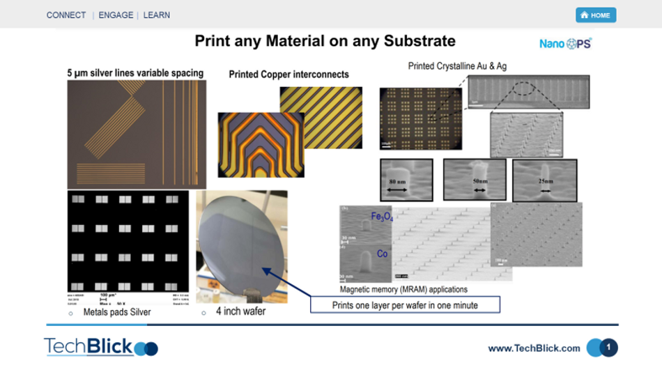
Nano-Ops has shown that all types of materials can be deposited using various directed assembly techniques (electrophoretic and fludic). Slides one and two below shows example of different materials and patterns deposited on an patterned wafer (on the template wafer) using this technique. The feature sizes range from a few mironmeters down to 20 nanometers.
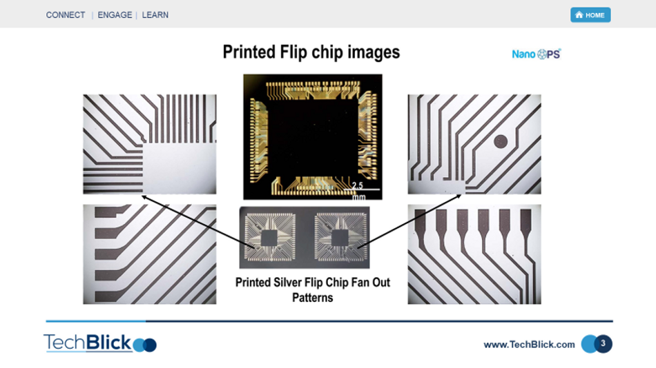
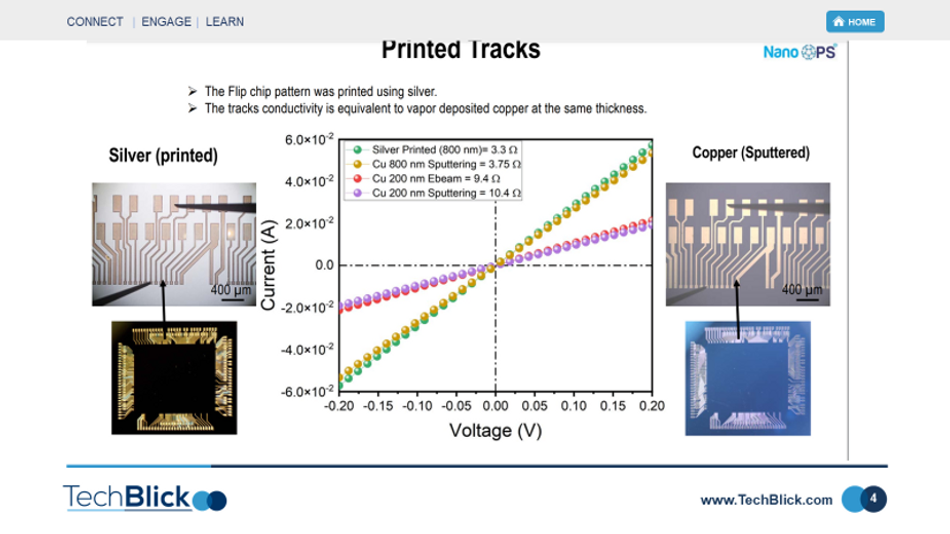
In slides three and four show an example of a fan-out circuit printed. The gold structure are 12um feature. The thicknesses are typically between 300nm and 1um with upto 50% of bulk conductivity achieved on the inked wafer. Indeed, as seen in slide 4, the I-V characteristics of the 800nm-thick 'printed' Cu lines are comparable to that of 800nm sputtered Cu lines.
This is a unique technique full of potential. When the entire process (directed assembly + alignment + transfer + consistency across multiple print runs ) is optimized for a given material set and layer structure in a given application, then it could lead to rapid 'printing' of nanoscale complex multiplayer and multi-material devices at costs far below standard silicon fabs and at resolutions far beyond the reach of stnadard printing techniques.
Ahmed et al will be showcasing and presenting this technology in Eindhoven on 12-13 OCT 2022 at the TechBlick show. Learn more here https://www.techblick.com/electronicsreshaped
Read more at https://www.techblick.com/post/additive-and-high-throughput-nanoscale-multi-layer-printing-materials-and-devices-on-any-substrate