Circuit Card Assemblies: A Comprehensive Guide
Circuit card assemblies (CCA) give birth to a complete printed circuit board (PCB) after assembling every component. A printed circuit board has no electrical components and needs to go through a manufacturing process called circuit card assemblies which are the complete board assembly.

Last updated on 11 Apr, 2024. 14 minutes read
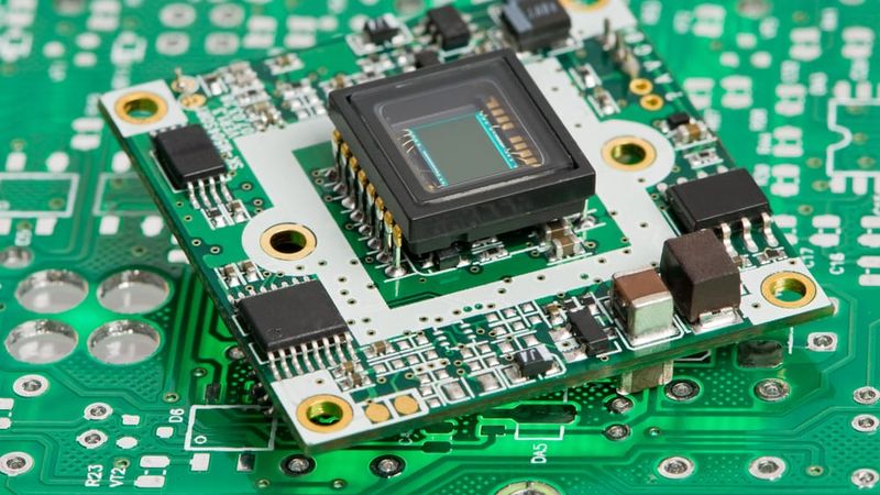
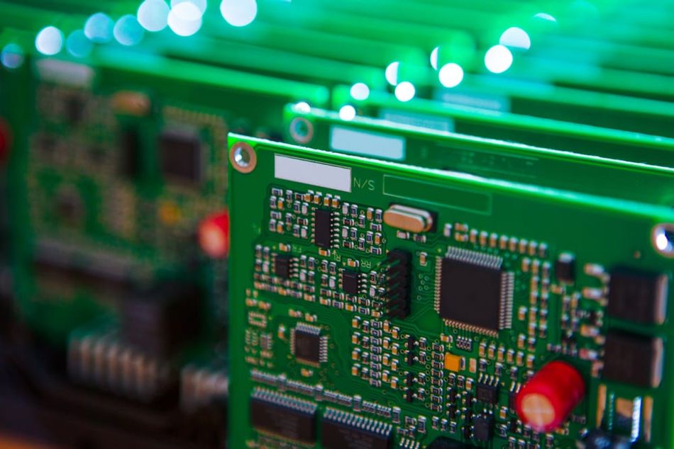
Assembled integrated microcircuit board
Introduction
Circuit card assemblies (CCAs) are the backbone of modern electronics, enabling the creation of compact, high-performance devices. These intricate assemblies, featuring printed circuit boards (PCBs) populated with electronic components, have transformed the engineering landscape by pushing the boundaries of miniaturization and functionality.
CCA technology has been instrumental in the development of increasingly sophisticated electronic systems, ranging from consumer gadgets to critical aerospace and medical equipment. This post will discuss the components, types, manufacturing process, advantages, and challenges related to Circuit Card Assembly.
Essential Components of a Circuit Card Assembly (CCA)
A circuit card assembly has several aspects that enable proper circuit functionality. These can be broken down into three essential components.
Printed Circuit Board (PCB)
Electronic Components
Connectors
Printed Circuit Board (PCB)
Circuit assembly features in all electronic devices, and the PCB provides the basic platform for the assembly and wiring of electronic components. The PCB features several key elements. The following four components are essential for basic circuit assembly.
Substrate - It is the foundation of a circuit assembly that holds all electrical components in place. Substrate materials vary based on PCBA type, such as flexible, rigid, or metal core boards. Mostly, fibreglass is used in rigid PCBs while Polyimide is a common material for flexible PCBs.
Copper Traces - Copper traces provide conductive paths to connect different PCB components. Circuit card assembly substrate and copper foil are laminated together using heat. Depending on PCB layers, multiple copper layers may be etched according to the circuit schematic.
Solder Mask - It is a thin protective layer that covers the conductive parts of the circuit to prevent corrosion and reduce the risk of solder shorts. It also helps the manufacturers accurately place the components on the PCB.
Silkscreen - It is the topmost PCB layer featuring the essential symbols, values and text. The Silkscreen makes it easier for the user to understand the placement and functionality of the PCB.
Recommended Reading: PCBA vs PCB: The foundation of modern-day electronics
Electronic Components
The electronic components are the workhorses in a circuit card assembly. The placement of these components is a critical aspect of the optimized design and performance of the circuit. While there are many electronic components in a CCA, you will find the following components in almost any assembly.
Diode - A two-terminal semiconductor that allows unidirectional current flow, mainly used for rectification and voltage regulation.
Resistor - Most commonly used component in a circuit card assembly, responsible for providing current flow opposition. Almost no circuit card assembly is complete without a resistor and it’s available in through hole and surface mount technologies.
Transistors - Primarily used for switching applications, transistors are three-terminal components in a CCA. They are available in BJT and FET types and are a critical part of circuits that interface with external devices like actuators, and sensors.
Inductors - Two-terminal passive components used for energy storage in the form of a magnetic field. They have immense applications in power electronic circuits.
Capacitors - Two terminal devices that store energy electrostatically in an electric field. They are also used for blocking direct current and many filtering applications.
Further Reading: Components of a PCB: A Comprehensive Guide
Connectors
Connectors are a critical part of circuit cards. They ensure connectivity between the card and external components, allowing signals to flow smoothly to and from the circuit. The connectors interface the circuit card assembly and external devices like PCBs, sensors, or other components.
Other than connectivity, these components are also responsible for power distribution. For instance, the connector on the smartphone PCBs allows the battery to be charged.
Based on their use, there are several types of connectors such as:
Board-to-Board Connectors - Connect two PCBs. These are often needed in systems where a circuit board needs to communicate with two or more PCBs. For instance, embedded systems connect with various sensor modules via dedicated connector pins.
I/O Connectors - Input Output (I/O) connectors interface the CCA with external components. They are used for data or power transmission. For instance, USB, HDMI and Ethernet connectors are some examples of I/O connectors.
Wire-to-Board Connectors - These connectors provide connectivity between wires from sensors, actuators, and the PCB. These connectors are designed to handle the flexibility of wires without signal disruption.
High-Frequency Connectors - Used for connecting radio frequency and microwave signals. The connectors ensure minimal signal loss, thanks to various elements like dielectrics, tight tolerance, and advanced shielding.
FPC/FFC Connectors - FPC (Flexible Printed Circuit) and FFC (Flexible Flat Cable) connectors cater to flexible electronic components. FPC connectors link thin, flexible PCBs, while FFC connectors connect ribbon-like, extremely thin, and flexible flat cables.
Suggested Reading: Types of PCB Connectors: An In-Depth Guide
CCA Manufacturing Process
Circuit Card Assembly manufacturing is a multi-stage process. This section will discuss. Here is a quick look:
PCB Fabrication
The process starts with the creation of the printed circuit board using photomasks. It features a series of processes such as
PCB etching
Drilling
Plating processes to form the conductive traces and vias
Solder Paste Application
The solder paste is applied to the exposed pads of the PCB using a stencil. A thin stainless steel stencil covers the PCB. The solder paste is composed of tiny metal balls, is primarily 96.5% tin, 3% silver, and 0.5% copper, and it's lead-free.
The solder is combined with Flux for solder melting and adhesion. Advanced CCA lines employ mechanical devices and printing machines to hold the PCB and stencil in place, applying solder paste precisely to designated areas. Following stencil removal, the paste remains in position.
In solder pasting machines, an additional solder paste inspection process checks for accurate solder placement, shape, size and thickness of the solder paste.
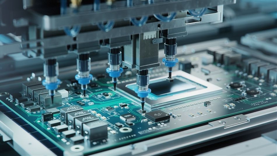
 Fig 2: A laser-cut stainless steel stencil for solder paste application Component Placement
An automated pick-and-place machine is guided by computer-aided design (CAD) files, allowing it to position the surface-mount components onto the solder paste-coated pads. Traditionally, the process was done manually but modern machines reduce the workload by swiftly placing the components and reducing operational time.
These machines allow PCB production in bulk, thanks to precise and reliable component placement.
Reflow Soldering
Once the components are accurately placed, the PCB is heated up to 250 degrees Celsius. It causes the solder paste to melt, which forms a permanent connection between the exposed PCB pads and the SMD components.
In double-sided CCAs, the stencilling and reflow process is repeated for each side. The side with the fewest pieces and stencils is stencilled, placed, and reflown first.
Through-Hole Component Insertion
Following CMD component mounting, the through-hole components are inserted into the designated holes. It may be an optional step considering that most modern PCBs feature SMD components only.
Typically, modern pick-and-place robots can insert the components accurately, but the process is carried out manually in many assembly plants.
Wave Soldering
In this step, the through-hole components are soldered to the PCB. The PCB is passed over a molten solder wave to fill the through-holes and create a strong bond between the component leads and the PCB.
Inspection and Testing
The CCA undergoes rigorous inspections and tests, such as automated optical inspection (AOI), X-ray inspection, and in-circuit testing (ICT). In many cases, the PCB movement during the reflow process causes connection losses. Moreover, there can be a shortage of components or misplaced components.
Hence, inspection and quality control ensure that the PCB has achieved the desired state before it is sent for packaging. Based on the PCB type, there can be several visual and in-circuit testing processes to ensure PCB quality.
Suggested Reading: Flying Probe Test: An Extensive Guide to the Technology and Applications
Conformal Coating and Packaging
Depending on the application, the CCA may receive a protective conformal coating or be encapsulated in resin for added protection against environmental factors and mechanical stress.
The CCA is then mounted into an enclosure, connected to other system components, and packaged for shipment to the end-user.
Types of Circuit Card Assembly
Circuit Card Assembly has three major types. Here is a quick look:
Box Build Assembly
Box build assemblies are also called systems integration. It refers to a basic PCBA or CCA housed in an enclosure. So, a typical box-build assembly includes both electronic and electromechanical parts such as:
Connectors, modular connectors
Batteries, and other power sources
Custom cable assemblies
Heatsinks and other thermal attachments
Board attachments like brackets, and standoffs
Since the box is part of the system design, its enclosure is also specially designed according to the PCBA. Since box-build assemblies are virtually complete systems, they are more robust and profitable.
Surface Mount Technology (SMT) Assembly
Surface Mount Technology (SMT) refers to applying electronic components directly onto the surface of the PCB. The process enables compact PCB creation and promotes automation.
The components don’t need to be inserted into through holes, as they are soldered directly on the metal pads on the PCB surface. Therefore, SMT can produce more complex and compact circuits leading to the production of high-density PCBs.
The process is highly configurable, so it’s the ideal option for high-volume production. SMT uses techniques like Ball Grid Array (BGA) for securing devices on the PCB surface.
Recommended reading: SMT Manufacturing: Everything You Need to Know
Through-Hole Assembly
Through-hole assembly refers to PCBs that contain drilled holes to allow the component leads to pass through. The leads are then soldered on the other side of the PCB. Through-hole assembly evolved from single-sided to double-sided, and finally to multi-layer boards.
With the introduction of SMT assembly, through-hole assembly may have lost some of its popularity but it’s still widely used in applications where components don’t support SMT assembly. For instance, transformers, and electrolytic capacitors require through-hole assembly.
Advancements in CCA Technology
CCA technology has come a long way since its inception. Over the years, the following advancements have revolutionized the design concepts for CCAs.
High-Density Interconnect (HDI) PCBs
High-Density Interconnect (HDI) PCBs enable the compact CCA design for , high-performance electronic devices. They offer numerous benefits, such as:
Increased component density
Improved signal integrity
Reduced signal propagation delay
HDI focuses on employing smaller via sizes, finer trace widths, and tighter spacing, allowing more components in a smaller footprint, and making them essential for applications requiring miniaturization and high functionality.
HDI technology is crucial in various industries where compact, high-performance electronics are essential:
Consumer electronics - Smartphones, tablets, and wearable devices.
Medical devices - Development of smaller, more reliable, and less invasive implantable electronics and diagnostic equipment.
Aerospace and defense - Used in avionics, radar systems, and satellite communications, where high-density packaging and reliable performance are critical.
To successfully implement HDI technology in CCA design, engineers must adhere to specific design rules and guidelines covering aspects such as:
Minimum via size, pad size, and spacing
Trace width and spacing requirements for different signal types and impedance control
Incorporation of micro vias for higher routing density and improved signal integrity
3D Packaging Techniques
3D packaging techniques, such as package-on-package (PoP) and through-silicon via (TSV), also promote miniaturization, higher component density and improved performance. These techniques allow for the vertical stacking of multiple integrated circuits (ICs) or packages, resulting in more efficient space utilization and enhanced functionality.
Package-on-package (PoP) involves stacking two or more packages on top of each other, with each package containing one or more ICs. The packages are interconnected using solder balls or bumps, enabling communication between the stacked devices.
This technique is particularly useful for integrating multiple functionalities, such as combining memory and logic devices in a single package offering the highest level of 3D integration and enabling the creation of highly compact and high-performance 3D ICs
Implementing 3D packaging techniques in CCA design requires addressing several technical challenges:
Thermal management - The increased power density in stacked devices can lead to higher operating temperatures, necessitating efficient heat dissipation strategies like thermal interface materials and optimized package designs.
Signal and power integrity - 3D packages require advanced modelling and simulation techniques to ensure optimal signal and power integrity.
Manufacturing - Precise alignment and bonding techniques, specialized packaging equipment, and materials are essential for reliable 3D package manufacturing.
Testing and inspection - Advanced techniques like 3D X-ray inspection and 3D computed tomography (CT) are employed to detect defects and ensure the integrity of 3D interconnects. Design-for-testability (DFT) principles must be incorporated into the 3D package design to facilitate effective testing and debugging.
Advanced Materials for CCAs
Advanced materials, such as high-temperature laminates and low-loss dielectrics, are critical CCA designs for thermally stable electronic systems.
High-temperature laminates are made from materials such as: *
Polyimide
Bismaleimide triazine (BT
Cyanate ester,
These materials offer superior thermal stability, glass transition temperature (Tg), and decomposition temperature (Td) compared to traditional FR-4 laminates. These laminates are essential for applications operating in extreme environments, such as aerospace, automotive, and oil and gas industries.
Recommended Reading: What are Circuit Boards Made Of? An Extensive Guide to Materials and Manufacturing Processes
Low-loss dielectrics, characterized by low dielectric constant (Dk) and low dissipation factor (Df), are crucial for high-speed, high-frequency applications. For instance, polytetrafluoroethylene (PTFE), liquid crystal polymer (LCP), and hydrocarbon ceramic laminates minimize signal loss, reduce signal distortion, and improve signal integrity in high-speed digital circuits.
Property | Traditional FR-4 | High-Temperature Laminates | Low-Loss Dielectrics |
Glass Transition Temp. (Tg) | 130-140°C | 200-250°C | 280-320°C |
Decomposition Temp. (Td) | 300-320°C | 350-400°C | 400-450°C |
Dielectric Constant (Dk) | 4.2-4.5 | 3.8-4.2 | 2.2-3.5 |
Dissipation Factor (Df) | 0.02-0.03 | 0.01-0.02 | 0.001-0.005 |
Thermal Conductivity | 0.3-0.4 W/mK | 0.4-0.7 W/mK | 0.2-0.3 W/mK |
Moisture Absorption | 0.1-0.3% | 0.05-0.1% | 0.01-0.05% |
The table compares the properties of traditional FR-4 laminates with high-temperature laminates and low-loss dielectrics. Advanced materials exhibit superior thermal stability, lower dielectric constant and dissipation factor, better thermal conductivity, and lower moisture absorption, contributing to improved reliability and performance in demanding environments.
Challenges and Considerations in CCA Design and Manufacturing
Thermal Management
Thermal management poses a critical challenge for high-density circuit card assemblies (CCAs). As component density and power consumption increase, the heat generated within the assembly rises, leading to potential issues such as component overheating, reduced performance, and decreased reliability.
Moreover, the limited space available for heat dissipation in high-density CCAs is a primary concern. Closely packed components and advanced packaging techniques, like 3D packaging and multi-chip modules (MCMs), further concentrate heat sources, exacerbating thermal challenges.
To address these challenges, various thermal management techniques are employed in CCA design:
Heat Sinks - Passive cooling devices made from high thermal conductivity materials like aluminium and copper. They dissipate heat from components to the surrounding environment through their large surface area to maximize heat transfer.
Thermal Vias - Conductive paths that transfer heat from components to the PCB's outer layers or dedicated thermal planes. Strategically placing thermal vias near high-power components provides a low-resistance path for heat dissipation.
Thermal Simulation and Design Optimization - Thermal simulation software, such as computational fluid dynamics (CFD) tools, allows designers to model heat transfer and airflow within the CCA. By simulating various design scenarios, engineers can identify hot spots, evaluate the effectiveness of different cooling techniques, and optimize the placement of components and thermal management features.
Thermal Interface Materials (TIMs) - TIMs, such as thermal greases, pads, or adhesives, improve the thermal contact between components and heat sinks, reducing the thermal resistance at the interface.
Forced Air Cooling - Active cooling methods, like fans or blowers, enhance airflow and heat dissipation in CCAs. Forced air cooling is particularly effective for high-power applications or when the ambient temperature is high.
Liquid Cooling - For extreme high-power applications, liquid cooling systems, such as cold plates or immersion cooling, provide more efficient heat removal compared to air cooling methods.
Recommended Reading: Guide to PCB Mounting: Techniques, Tips, and Best Practices
Ensuring Signal Integrity
Maintaining signal integrity and minimizing electromagnetic interference (EMI) are crucial aspects of circuit card assembly (CCA) design. As operating frequencies and data rates increase, the challenges associated with signal integrity and EMI become more pronounced. Poor signal integrity can lead to data corruption, timing errors, and system malfunctions, while excessive EMI can cause interference with other electronic devices and violate regulatory requirements.
Signal integrity refers to the ability of a signal to maintain its intended characteristics, such as amplitude, timing, and shape, as it propagates through the CCA. Factors that can degrade signal integrity include:
Impedance mismatches
Reflections
Crosstalk
Power supply noise
To ensure proper signal integrity, designers must carefully consider the following aspects.
Impedance Matching - Using techniques like controlled impedance routing, termination networks and differential signalling ensures consistent characteristic impedance throughout the signal path.
Crosstalk Reduction - Increasing trace spacing, and guard traces, optimizing routing topology and using differential signalling to reduce crosstalk
Reducing Electromagnetic Interference
Minimizing EMI ensures proper functioning of the CCA and compliance with electromagnetic compatibility (EMC) regulations. EMI can be generated by various sources within the CCA, such as high-speed digital circuits, switching power supplies, and clock signals. To reduce EMI, designers must implement appropriate shielding and grounding techniques:
Shielding - Enclosing sensitive components or circuits within a conductive enclosure to prevent the emission or reception of electromagnetic energy. Shielding materials, such as metal cans, conductive gaskets, or conductive coatings create a barrier against EMI.
Grounding - Providing a low-impedance path for high-frequency noise and preventing the coupling of EMI into sensitive circuits. Techniques such as the use of ground planes, split ground planes, and stitching capacitors can be employed to create an effective grounding network.
Conclusion
Circuit card assembly (CCA) technology has transformed electronics, enabling compact, high-performance devices across industries. CCAs, crucial for complex systems from consumer electronics to aerospace, offer unprecedented functionality and reliability in smaller form factors. Advances like high-density interconnect (HDI) PCBs and 3D packaging techniques drive innovation, expanding design possibilities and enhancing device capabilities.
As demand rises for smaller, faster electronics, CCA technology's significance grows. Future trends include component miniaturization, advanced packaging, and integration of technologies like 5G and IoT. Yet, these advancements pose challenges in design, manufacturing, and reliability. Engineers must innovate and adapt, leveraging tools and processes for high-quality, reliable CCAs. Continued CCA development promises profound impacts, fueling innovation and shaping the future of electronics across industries.
Frequently Asked Questions
What are the main components of a circuit card assembly (CCA)?
A circuit card assembly typically consists of a printed circuit board (PCB), electronic components such as integrated circuits, resistors, and capacitors, and connectors that allow the CCA to interface with other parts of the electronic system.
What are the benefits of using high-density interconnect (HDI) PCBs in CCAs?
HDI PCBs offer several benefits, including increased component density, improved signal integrity, and reduced signal propagation delay. By utilizing smaller via sizes, finer trace widths, and tighter spacing, HDI PCBs enable the integration of more components in a smaller footprint, making them ideal for applications that require miniaturization and high functionality.
How do 3D packaging techniques improve CCA performance?
3D packaging techniques, such as package-on-package (PoP) and through-silicon via (TSV), enable the vertical stacking of multiple integrated circuits or packages, allowing for more efficient use of space and enhanced functionality. These techniques provide shorter interconnects between components, leading to improved electrical performance, reduced power consumption, and faster signal transmission.
What are the main challenges in manufacturing high-density CCAs?
The main challenges in manufacturing high-density CCAs include achieving high component placement accuracy and maintaining soldering quality. The tight spacing between components and the reduced pitch of component leads require precise placement and soldering processes to avoid defects such as shorts, opens, or compromised solder joints. Manufacturers must employ advanced equipment, process control, and quality assurance measures to overcome these challenges.
How do engineers ensure signal integrity and minimize electromagnetic interference (EMI) in CCAs?
Engineers employ various techniques to ensure signal integrity and minimize EMI in CCAs. These include proper PCB layout and routing, impedance matching, crosstalk reduction, and the use of shielding and grounding techniques. Signal integrity analysis tools and EMI simulation software are used to model and optimize the design before fabrication. Adherence to best design practices and guidelines is crucial for achieving optimal signal integrity and EMI performance in CCAs.