Buck Converters: A Comprehensive Guide for Hardware Design Engineers
A complete technical guide to buck converters covering operating principles, CCM and DCM, synchronous vs. asynchronous designs, component selection, control methods, PCB layout, and common troubleshooting issues.

31 Mar, 2026. 13 minutes read
Key Takeaways
- The duty cycle directly determines the output voltage of a buck converter via the principle of volt-second balance: D = Vout/Vin [2].
- Inductor value and capacitance control ripple and stability. Higher inductance reduces ripple but slows transient response; low-ESR capacitors minimize voltage ripple [1].
- Continuous conduction mode (CCM) gives predictable transfer characteristics; discontinuous conduction mode (DCM) occurs at light loads and changes the voltage conversion ratio [2].
- Synchronous converters replace the diode with a MOSFET for higher efficiency, especially at low output voltages [3].
- Control methods vary: voltage-mode control is simple, current-mode provides better transient response, and constant on-time control offers ultra-fast response but generally variable frequency [4] [5].
- Good PCB layout is critical: place capacitors close to the IC, minimize high-di/dt loops, keep analog and power grounds planes separate, and join them at a single star point [8].
- Troubleshooting involves checking for ripple, start-up issues, poor regulation, instability, and efficiency problems. Systematically isolate variables and verify component values [9].
Introduction
Modern electronics, especially in automation, run on many different voltages — a microcontroller might need 3.3V, its RF frontend 1.8V, and its power amplifier 5V — yet the available supply is rarely any of these. A 12V car battery, a 24V industrial bus, a single-cell lithium battery at 4.2V: the voltage you have and the voltage you need are rarely the same. Solving this mismatch is one of the most common problems in electronic system design.
A linear regulator works, but at a cost, often requiring bulky heatsinks. It simply drops the excess voltage across a pass transistor, turning the difference into heat. Step down from 12V to 3.3V at 1A, and you are dissipating over 8W as waste heat. That is acceptable in low-power or cost-sensitive designs, but it becomes untenable when efficiency, battery life, or thermal budget are at issue.
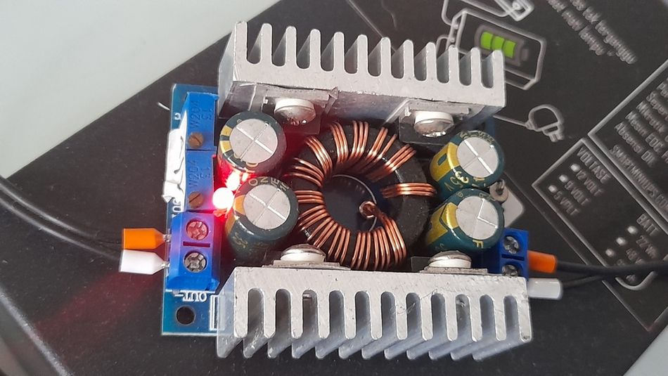
Switch-mode DC-DC converters are fundamental building blocks of modern DC power supply units. They efficiently generate voltage rails that differ from the supply using energy storage elements and high-frequency switching. Among them, the buck converter (step-down converter) is perhaps the most widely used. It solves the same problem without the waste. By rapidly switching the input voltage and filtering it through an inductor and a capacitor, it transfers energy to the output with typical efficiencies of 90–98%. No significant heat is generated, the components are compact, and the output voltage is precisely controlled by adjusting how long the switch stays on each cycle.
This article covers everything you need to understand and design with buck converters, including a practical 12V-to-3.3V at 5A design example, CCM vs DCM, synchronous vs asynchronous comparison, control methods, PCB layout best practices, troubleshooting, and a buck vs boost vs buck-boost comparison table.
What Is a Buck Converter?
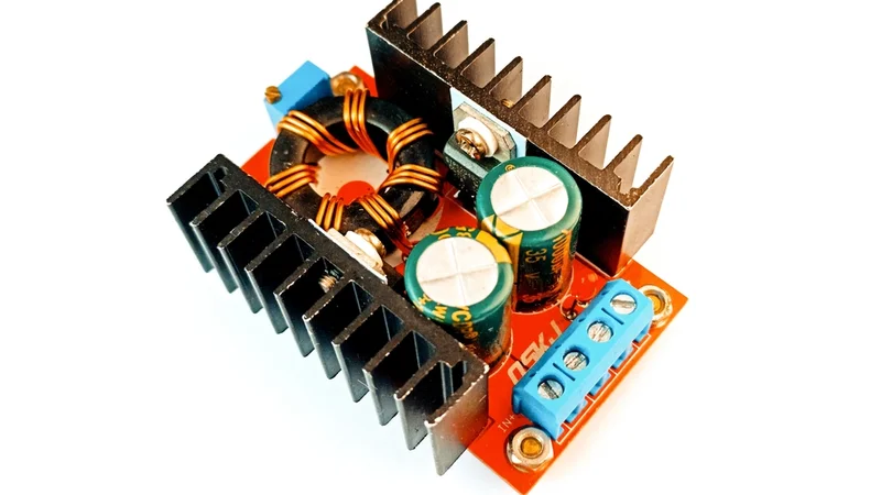
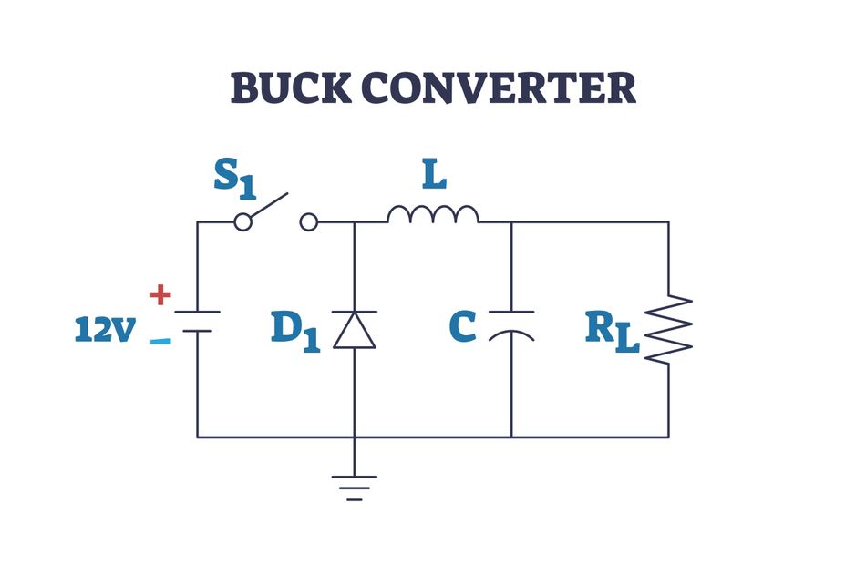
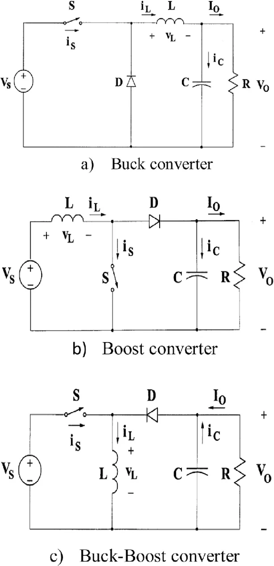
A buck converter is also known as a step-down converter. It converts a high voltage to a lower-voltage output from a given voltage source. A basic buck converter circuit consists of a high-side switch (MOSFET or IGBT), a low-side diode (or MOSFET in synchronous versions), an inductor L, and input and output capacitors [1].
When the high-side switch is ON, the input voltage minus the output voltage is applied across the inductor. This forward voltage causes the inductor current to ramp up linearly, storing energy in its magnetic field and delivering output current to the load simultaneously. When the switch is OFF, the inductor opposes the change in current and forward-biases the diode, allowing current to continue flowing into the load, with the inductor current ramping down as its stored energy is depleted. The inductor current, therefore, has a triangular waveform, and the output capacitor, with its associated impedance, smooths this into a nearly steady DC voltage with a small residual ripple.
In a steady state, the average voltage across the inductor must be zero; this is the principle of volt-second balance [2]. The ON state lasts for T_ON = D x T_S, and the OFF state lasts for T_OFF = (1 - D) x T_S. Equating the volt-seconds for each state yields:
Vout = D x Vin - (switch and diode drops)
For ideal switches, the duty cycle directly determines the output voltage. Designers adjust the duty cycle by modulating the switch's on-time to regulate Vout.
Circuit Analysis: Volt-Second Balance and Inductor Ripple Current
ON State
The switch connects the inductor to Vin. The applied inductor voltage is Vin - Vout. The inductor current increases linearly:
ΔIL(+) = (Vin - Vout) x T_ON / L
OFF State
The switch is off, and current flows through the diode. The voltage across the inductor is approximately -Vout. The current decreases linearly:
ΔIL(-) = Vout x T_OFF / L
Ripple Current
Using T_ON = D/fs and T_OFF = (1 - D)/fs:
ΔIL= (Vin - Vout) x D / (L x fs)
where fs is the switching frequency. Note that ripple is maximised at D = 0.5 and is independent of load current — it is purely a function of circuit parameters.
Peak Current
The inductor peak current is: I_PEAK = I_LOAD + ΔIL/ 2
Select the inductor so that its saturation current rating exceeds I_PEAK. Larger inductance reduces ripple but increases size and cost.
Input Capacitance
C_IN >= (I_LOAD x D) / (delta_VIN x fs)
Use low-ESR ceramic capacitors placed near the VIN and ground pins. Add a 0.1 uF capacitor in parallel for high-frequency decoupling. The input capacitor must also be rated for the RMS ripple current, which is approximately I_LOAD × √(D × (1−D)).
Output Capacitance
C_OUT >= delta_IL / (8 x fs x delta_VOUT)
In practice, output voltage ripple has two components: the capacitive ripple (above) and the resistive ripple due to ESR:
ΔVOUT(ESR) = ΔIL × ESR
The dominant term determines total ripple. Choose capacitors with low ESR to minimise both components [8].
Recommended Reading: How Switching Regulators Work: A Deep Dive for Power Engineers
Continuous vs Discontinuous Conduction Modes (CCM vs DCM)
The inductor current waveform is the key to understanding how a buck converter behaves under different load conditions. Depending on how much current the load draws, the converter will operate in one of two fundamental modes, and the distinction has significant consequences for efficiency, control, and output regulation.
Continuous Conduction Mode (CCM)
In CCM, the inductor current never reaches zero. It ramps up during the ON state and ramps down during the OFF state, but always remains positive. This is the normal operating condition at moderate to high loads, and it is the mode most control loops are designed around. The conversion ratio is clean and load-independent:
Vout = D × Vin
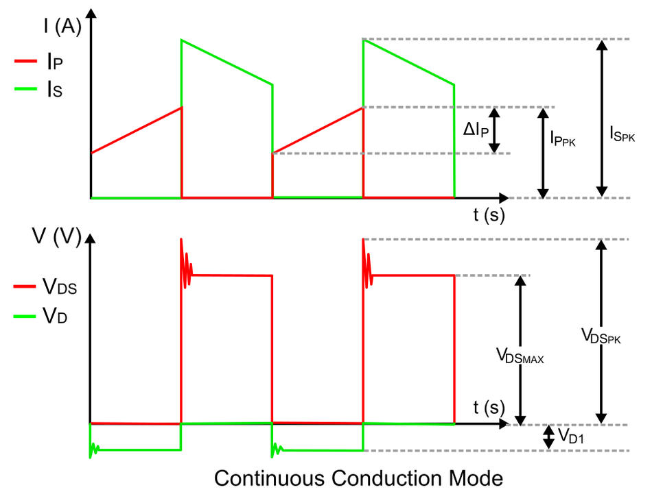
CCM offers low peak currents relative to average load current, low output ripple, and predictable small-signal behavior — all of which simplify compensation and closed-loop design.
Discontinuous Conduction Mode (DCM)
As load current decreases, the ripple current stays constant while the average inductor current falls. Eventually, the valley current reaches zero — this is the CCM/DCM boundary. In a non-synchronous converter, the diode blocks negative current, so once the inductor current hits zero it stays there for the remainder of the switching cycle. This idle period is DCM's defining third state.
In DCM, the conversion ratio becomes load-dependent, impacting voltage regulation.
M = Vout/Vin = (1 + √(1 + 4D²/K)) / 2
where K = 2L·fs/R is the conduction parameter, and R is the effective load resistance. Because M now varies with load, a control loop designed purely for CCM will allow the output voltage to rise at light loads if it cannot respond fast enough — a common source of overvoltage in poorly compensated designs [2].
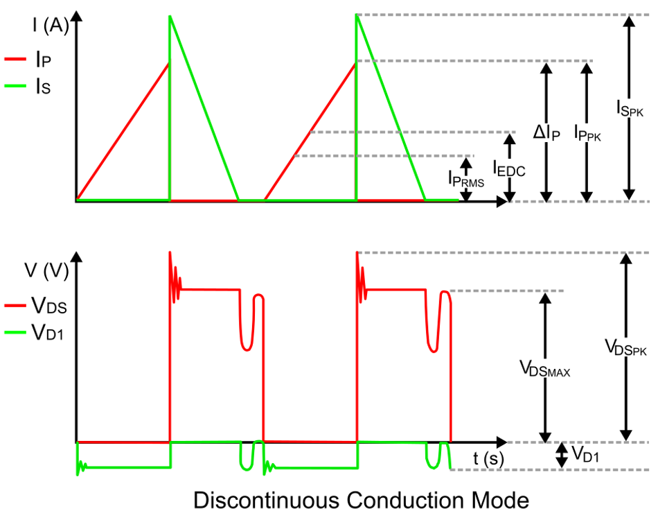
At very light loads, it reduces switching losses and can improve overall efficiency. However, it raises peak currents, increases output ripple, and complicates control design.
The CCM/DCM Boundary and Critical Inductance
The boundary occurs when the valley inductor current just touches zero, i.e., when the load current equals exactly half the peak-to-peak ripple. The minimum inductance required to maintain CCM down to a specified minimum load current I_LOAD_MIN is:
L_CRIT = (Vin − Vout) × D / (2 × I_LOAD_MIN × fs)
Choosing L > L_CRIT guarantees CCM operation above I_LOAD_MIN. In practice, designers add margin, since component tolerances and temperature variation shift the boundary.
Synchronous vs Asynchronous Buck Converters
Asynchronous (Diode-Based)
In asynchronous buck converters, a diode is the low-side switch. The diode's forward voltage drop (0.3 to 0.5 V for a Schottky at 1 A) causes significant conduction loss. At large step-down ratios, the diode conducts for most of the cycle, further reducing efficiency. Asynchronous converters are less expensive and handle light loads well because the diode naturally prevents reverse current.
Synchronous (MOSFET-Based)
In synchronous buck converters, a low-side MOSFET replaces the diode. The control IC drives both high-side and low-side FETs with dead time to prevent shoot-through. Because MOSFETs have low on-resistance, synchronous designs achieve higher efficiency [3]. They can operate in forced CCM to maintain constant frequency or enter pulse-skipping mode at light loads. Trade-offs include higher cost, increased driver complexity, and potential for shoot-through.
Selection Criteria
Choose asynchronous regulators for simple, low-cost, or noise-sensitive systems. Choose synchronous designs when efficiency and current capability are critical [3].
Component Selection: 12 V to 3.3 V at 5A Design Example
Duty Cycle Estimate
D = 3.3 / 12 = 0.275. Accounting for MOSFET on-resistance and diode drop, assume D = 0.28.
Selecting the Inductor
Target 30% ripple current: ΔIL = 0.3 x 5 A = 1.5 A
This is a standard starting point — reducing ripple improves output quality but demands a larger inductor; increasing ripple reduces inductance but raises peak current stress.
At 500 kHz switching frequency:
L = (Vin − Vout) × D / (ΔIL × fs) = (12 − 3.3) × 0.28 / (1.5 × 500,000) ≈ 3.3 µH
Select a standard value of 3.3 µH or 4.7 µH and verify against the target IC's recommended range.
Select an inductor rated above 6 A saturation current (I_LOAD + ΔIL/2 = 5 + 0.75 A) and apply a 20–30% margin above I_PEAK to handle transients.
Input Capacitor
To limit input ripple to 100 mV:
C_IN >= (5 A x 0.28) / (0.1 V x 500,000) = approximately 28 uF
Place two to three 10 uF ceramic capacitors directly at the VIN and GND pins, rated at 25 V for a 12 V input, plus a 0.1 µF in parallel for high-frequency decoupling.
Output Capacitor
For 30 mV output ripple (0.9% of 3.3 V):
C_OUT >= 1.5 A / (8 x 500,000 x 0.03 V) = approximately 12.5 uF
Note that this formula assumes negligible ESR. In practice, ESR adds a resistive ripple component — ΔVOUT(ESR) = ΔIL × ESR — and the larger term dominates the total ripple. Start with a 22 µF low-ESR ceramic capacitor and add a 47 µF if transient response demands it. Check the IC datasheet for ESR requirements — some controllers need a minimum ESR for loop stability; others do not.
MOSFETs and Diodes
For synchronous designs, choose MOSFETs with low on-resistance and gate charge. Ensure drain-source voltage rating exceeds 12 V plus margin. For asynchronous designs, use a Schottky diode with a low forward voltage (0.3 V) and a current rating above 5.75 A.
Buck-Boost Converter Overview
A buck-boost converter can either increase or decrease the input voltage. It combines the functions of a buck and a boost: one switch-diode network acts as the buck converter, and another acts as the boost converter. This makes it essential in battery-powered systems where the supply voltage rises above and falls below the regulated output over the discharge cycle.
Basic Operation
During the first interval, one switch energizes the inductor, ramping the current up and storing energy in its magnetic field. During the second interval, the second device transfers the stored energy to the output, ramping the current down. In the classical single-inductor inverting topology, the output voltage is negative with respect to ground, though non-inverting versions using additional switches exist [6].
Four-Switch Buck-Boost
Modern integrated regulators implement a four-switch synchronous buck-boost using two high-side and two low-side MOSFETs sharing a single inductor. When the input voltage is higher than the output, the regulator disables one MOSFET and holds another on, so the remaining two switches regulate like a synchronous buck converter. When the input drops below the output, the roles reverse, and the circuit operates as a boost converter.
Advantages include no diode conduction losses, seamless buck/boost operation, and built-in short-circuit protection in boost mode. The trade-off is increased complexity and cost.
Control Methods
The control method determines how a buck converter's feedback loop responds to line and load disturbances. Each approach makes different tradeoffs between simplicity, transient performance, and frequency stability.
Voltage-Mode Control
The error amplifier senses only the output voltage, compares it to a reference, and drives a PWM comparator that adjusts the duty cycle to correct the error.
Pros: simple, high noise immunity.
Cons:. requires a type-II or type-III compensation network, slower transient response due to the single feedback path.
Current-Mode Control
An inner current loop measures the inductor current and compares it to the outer voltage loop error signal, turning the switch off cycle-by-cycle when the current limit is reached. Adding an inner current loop. Pros: faster transient response, simplified outer loop compensation, inherent cycle-by-cycle current limiting. Cons: susceptibility to noise on the current sense signal, requires slope compensation above 50% duty cycle to prevent sub-harmonic oscillation.
Constant On-Time (COT)
A comparator monitors the output voltage and triggers a fixed-duration on-pulse whenever Vout falls below the reference, then waits for the next threshold crossing. The switching frequency naturally adjusts to load and input voltage variations [4] [5].
Pros: very fast transient response, often requiring no traditional compensation network, simple loop.
Cons: variable frequency introduces jitter and EMI, and the topology requires sufficient output voltage ripple for the comparator threshold, either via natural ESR or an injected ripple signal.
Selection: Voltage-mode for fixed frequency and simplicity, current-mode for balanced performance, COT for ultra-fast transient response.
PCB Layout Best Practices
- Minimize the high-di/dt input loop first. Place the input capacitor as close as possible to the VIN and GND pins with short, wide copper traces or pours. This loop — VIN capacitor → high-side MOSFET → low-side MOSFET/diode → GND — carries pulsed current and generates voltage spikes via V = L × dI/dt. Minimizing its area minimizes radiated EMI and voltage stress [7].
- Place the inductor near the switch node. Keep the switch node copper area small to minimize radiated EMI.
- Place the output capacitor close to the inductor. Minimize loop area for good regulation and reduced ringing.
- Place small-signal components carefully. Feedback divider, compensation network, soft-start capacitor near the control IC, away from the switch node.
- Create a single-point ground. Separate analog (quiet) and power (noisy) grounds, connect at one point (typically at the IC's thermal pad) [8].
- Minimize hot loop perimeter. Use short, wide traces on a single layer for the high-di/dt loop.
- Use ground planes to shield sensitive signals and reduce inductance.
Common Troubleshooting Issues
Excessive output ripple: Inductor too small or output capacitor undersized/high ESR. Increase inductance or add capacitance. Also, check switching frequency — if the converter has entered DCM under light load, ripple will increase naturally. Verify the PCB layout minimizes the output loop area, as parasitic inductance adds effective ESR [9].
Failure to start: Check the enable pin logic level and input voltage — confirm it exceeds the UVLO threshold with margin. Excessive output capacitance can trigger hiccup-mode current limiting during soft-start; if so, increase the soft-start time via the soft-start capacitor or resistor.
Voltage present at the output when off: Leakage from another power domain feeding the output through a shared rail or load switch.
Power Regulation: Voltage drop along the power path or noise on the sense pin. Keep sense traces short.
Slow transient response: Excessive inductance or output capacitance slows the loop bandwidth. Reduce L or C, tighten the compensation, or switch to current-mode control for a faster inner loop.
Instability: Output capacitor ESR too low removes the ESR zero that stabilizes voltage-mode and some COT loops — verify ESR is within the datasheet recommended range.
Low efficiency: Identify the dominant power loss mechanism before changing components. High MOSFET R_DS(on) causes conduction loss proportional to I², and measures the MOSFET case temperature. High inductor DCR causes similar I² loss; check the inductor datasheet for DCR at operating temperature.
Temperature sensitivity: Electrolytic ESR increases at low temperatures. Use polymer or ceramic capacitors.
Comparison: Buck vs Boost vs Buck-Boost
Attribute | Buck (Step-Down) | Boost (Step-Up) | Buck-Boost |
Input/output relationship | Output less than input; D less than 1 | Output greater than input | Output can be above or below input |
Basic operation | Inductor between input and load | Inductor stores energy during ON state; releases it in series with input to output during OFF state | Combines buck and boost circuits |
Polarity | Same as input | Same as input | Same or inverted depending on topology |
Efficiency | High due to simple path | Moderate; higher switch stress | Lower than pure buck; four-switch versions minimize losses |
Complexity | Simple control and layout | More complex; careful inrush control | Complex; seamless mode transition needed |
Typical applications | CPUs, microcontrollers, sensors, analog rails | PFC, LED drivers, battery charging | Automotive, battery-powered devices, variable input |
Conclusion
This article covered everything you need to design and understand a buck converter, operating principles, CCM and DCM modes, synchronous and asynchronous topologies, component selection, control methods, PCB layout, troubleshooting, and a worked design example. A buck-boost overview and topology comparison round out the coverage.
FAQ
Q1. Why does the duty cycle equal Vout/Vin?
In a steady state, the average voltage across the inductor must be zero. The switch applies (Vin - Vout) for fraction D and the diode applies -Vout for (1 - D). Equating these volt-seconds yields D = Vout/Vin.
Q2. How do I choose the inductor value?
Determine the desired ripple current (20 to 40% of load current). Then use L = (Vin - Vout) x D / (fs x delta_IL). Larger L reduces ripple but increases size and slows transient response.
Q3. When would I use a synchronous converter?
When efficiency is critical, especially at high currents or large step-down ratios. The MOSFET replacing the diode lowers conduction losses. For low-cost or low-current applications, asynchronous may suffice.
Q4. What causes a buck converter to enter DCM?
When the load current falls below half of the inductor ripple current. This typically occurs at high switching frequency, which reduces ripple current and therefore raises the CCM/DCM boundary, or low input-to-output voltage differential, which reduces ripple current directly.
Q5. What is constant on-time control and when is it useful?
COT triggers a fixed on-pulse whenever Vout falls below the reference, varying the off-time naturally with load and line. It delivers a fast transient response without traditional compensation. Modern implementations use ripple injection to approximate fixed frequency. Best suited to fast-transient computing loads and low-quiescent-current battery applications.
Q6. How does a buck-boost converter differ from buck or boost?
A buck-boost can both step down and step up the input voltage. Four-switch implementations use synchronous MOSFETs to improve efficiency and provide continuous conduction across modes.
Q7. What layout mistakes can ruin a buck converter design?
The most damaging are: placing the input capacitor far from IC, long switch node traces, routing feedback near noisy nodes, merging analog and power grounds, and ignoring recommended ground connections. These cause jitter, EMI and poor regulation.
References
[1] Analog Devices, "DC to DC Buck Converter Tutorial," Analog Devices Technical Articles, Dec. 2025. [Online]. Available:Link
[2] E. Rogers, "Understanding Buck Power Stages in Switchmode Power Supplies," Texas Instruments, Application Report SLVA057, Mar. 1999. [Online]. Available:Link
[3] ROHM Semiconductor, "Differences between Synchronous and Nonsynchronous Rectifying DC-DC Conversion," ROHM TechWeb Switching Regulator Basics. [Online]. Available:Link
[4] ROHM Semiconductor, "Control Methods (Voltage Mode, Current Mode, Hysteresis Control)," ROHM TechWeb Switching Regulator Basics. [Online]. Available:Link
[5] Microchip Technology, "AN5629: Adaptive Constant-On-Time (ACOT) Control and Ripple Injection Circuit Design," Application Note DS00005629, 2021. [Online]. Available:Link
[6] L. Jiang, W. Ballar, A. Panigrahy, and H. Zhang, "Configuring Four-Switch Buck-Boost µModule Regulators for Versatile Applications: Step-Up, Step-Down, or Inverting Output," Analog Devices Technical Articles, Jan. 2026. [Online]. Available:Link
[7] Texas Instruments, "Five Steps to a Great PCB Layout for a Step-Down Converter," Application Report SLYT614, 2015. [Online]. Available:Link
[8] H. J. Zhang, "AN-136: PCB Layout Considerations for Non-Isolated Switching Power Supplies," Analog Devices (Linear Technology), Application Note AN136, Jun. 2012. [Online]. Available:Link
[9] EEPower, "Troubleshooting 9 Common DC-DC Buck Converter Issues," EEPower Technical Articles, Aug. 2024. [Online]. Available:Link
in this article
1. Introduction2. What Is a Buck Converter?3. Circuit Analysis: Volt-Second Balance and Inductor Ripple Current4. Continuous vs Discontinuous Conduction Modes (CCM vs DCM)5. Synchronous vs Asynchronous Buck ConvertersComponent Selection: 12 V to 3.3 V at 5A Design Example7. Buck-Boost Converter Overview8. Control Methods9. PCB Layout Best Practices10. Common Troubleshooting Issues11. Comparison: Buck vs Boost vs Buck-Boost12. Conclusion13. FAQ14. References