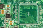
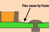
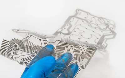
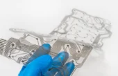
The popularity of wearable electronics has induced demand for their parts, including power sources such as triboelectric nanogenerators (TENGs). Such power sources must be both stretchy and high-performance, holding up under various deformation conditions over hours of use.
Semiconductors are the building blocks of modern electronics, powering everything from smartphones to satellites. This in-depth guide provides a comprehensive understanding of semiconductors' engineering principles and applications, delving into their fundamental concepts, materials, devices, manufacturing processes, and their impact on today's technology landscape.
This article provides a detailed examination of logic gate symbols, truth tables, and transistor level implementations, with practical insights for digital design and hardware professionals.
This article covers every aspect of the Arduino UNO pinout, presenting a technical, pin-by-pin explanation to help readers confidently design, analyze, and implement Arduino-based systems.
This article explores how to read resistor color code correctly, covering the fundamental theory, relevant standards, practical examples, and design-oriented insights, providing practical tips for efficient and accurate circuit prototyping.
Miniature RFID tags by Murata enable seamless system integration with durable, reprogrammable identification — delivering reliable tracking, authentication & traceability beyond the limits of traditional barcodes.
Learn why growing hardware teams slow down as they scale, and how aligned workflows, parallel collaboration, and real-time design visibility restore speed and momentum.
This article explores how to read resistor color code correctly, covering the fundamental theory, relevant standards, practical examples, and design-oriented insights, providing practical tips for efficient and accurate circuit prototyping.
Learn how to select the right Murata MLCCs for modern power architectures, balancing low ESL, stable capacitance, and smart placement to ensure power integrity in high-speed, high-current systems.
The popularity of wearable electronics has induced demand for their parts, including power sources such as triboelectric nanogenerators (TENGs). Such power sources must be both stretchy and high-performance, holding up under various deformation conditions over hours of use.
PCBA design capabilities are crucial to the future of wearable technology. Wearables and PCBA design are inextricably linked since both have a significant influence on each other. As wearable devices become more popular, electronics designers and manufacturers are designing smaller, denser, and more flexible devices.
Vias are small holes in a PCB that enable electrical connections between different layers of the board. In the context of PCB design, via tenting refers to the process of covering the vias with a protective layer, typically a solder mask or dry film. This protective layer shields the vias from environmental factors, such as dust, moisture, and chemicals, which can lead to corrosion or short circuits. As PCB technology continues to advance, the importance of via tenting in maintaining the performance and reliability of complex, high-density interconnect (HDI) and flexible PCB designs cannot be overstated. This guide explores the art and science of via tenting, shedding light on its significance, techniques, and applications in modern PCB design and manufacturing.
Researchers from ITMO University have come up with a new kind of wireless chargers – boxes with a uniformly distributed magnetic field inside them. Placing a device anywhere in the box will charge it, which makes the new technology stand out from its competitors, which can only ensure power transfer across short distances.
As an Inspiring 50 award-winner and startup founder, Greek-Albanian Sophia-Eriola Shanko is a first-time entrepreneur. She has a BSc in Control Systems Engineering, graduating in a classroom with two girls and 100 boys. She pursued a fully EU-funded MSc on Semiconductors and obtained her Ph.D. at TU Eindhoven.
‘Smart Circularity’—the circular economy as it relates to connected technology and the IoT—can help the world shift away from linear consumption to an economy where resources are fed back into a closed loop of recycling, reusing and sharing.
NANOWEB® is an extremely thin, transparent, conductive film that consists of an invisible, nanostructured metal mesh fabricated onto a glass or plastic surface. With its unrivaled transparency, conductivity, and flexibility, this patented functional film holds immense potential for both passive and powered use cases, with applications including electromagnetic interference shielding, antennas, 5G/6G redirection systems for elimination of dead spots, and deicing/defogging devices for vehicle windows and eyewear.
More than 20 years ago, a team set out to solve a problem: How do we reduce power loss and help reduce MOSFET size at the same time? LFPAK was the answer - and it changed everything.
Capacitors store electrical energy, similar to batteries, and are used in many electronic devices. Due to their voltage-storing nature, handling them can be dangerous. This article outlines various techniques and safety measures to safely discharge capacitors.
Manufacturing platform, Hubs, has published its Supply Chain Resilience Report 2023, featuring insights from 2022 and addressing recent supply chain disruptions, including the ongoing war in Ukraine, escalating tensions between China and Taiwan, and more. Download the full report below.
Learn the best methods and industry standards for cleaning circuit boards, removing contaminants like dust, flux residues, and corrosion to ensure optimal performance and longevity!