Via Tenting: A Comprehensive Guide to PCB Design and Manufacturing Techniques
Vias are small holes in a PCB that enable electrical connections between different layers of the board. In the context of PCB design, via tenting refers to the process of covering the vias with a protective layer, typically a solder mask or dry film. This protective layer shields the vias from environmental factors, such as dust, moisture, and chemicals, which can lead to corrosion or short circuits. As PCB technology continues to advance, the importance of via tenting in maintaining the performance and reliability of complex, high-density interconnect (HDI) and flexible PCB designs cannot be overstated. This guide explores the art and science of via tenting, shedding light on its significance, techniques, and applications in modern PCB design and manufacturing.

Last updated on 19 Oct, 2023. 14 minutes read
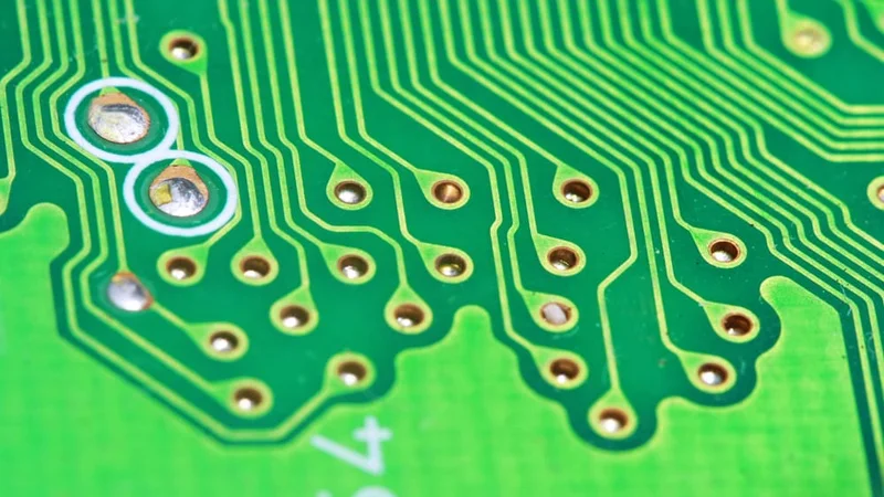
Via Holes on PCB
This article was first published on
www.wevolver.comIntroduction
Vias are plated through-holes on printed circuit boards (PCBs) that allow the transmission of electrical signals from one layer or side of the board to another. They offer protection from contaminants and enhance the overall reliability of the PCB. This makes them crucial for PCB manufacturing, especially for multilayer PCB assembly. Vias are usually copper-plated due to the conductivity of the material. PCB designers and manufacturers may prefer these holes either exposed or covered.
When the hole is completely closed, it is called a filled via or masked via, depending on the covering method. But when the hole is partly closed, the method applied is called tenting. Many PCB fabricators prefer the tenting method of covering the via. Covering vias with different materials allows them to conduct electrical signals while dissipating any produced heat. Tenting is not the only method available, but it is the most common one in PCB manufacturing. Tenting has both positive and negative impacts on PCBs, but to answer the question of whether or not you tent the vias on a PCB, the design and manufacturing requirements of the board, as well as the size of the via, hold the answer. Smaller vias are typically easier to fill or tent. When the via gets up to 15mil in diameter, it becomes too large for the tenting method.
Further reading: What is a Via?: A Comprehensive Guide.
Basics of Vias in PCB Design
Vias play a vital role in printed circuit board (PCB) design, serving as conduits for electrical connections between different layers of a board. They are small holes drilled into the PCB, typically filled with conductive material such as copper. There are three main types of vias: through-hole, blind, and buried.
Through-hole vias extend from the top layer to the bottom layer of the PCB, connecting all layers in the process. They are the most common type of via and are relatively easy to manufacture. However, they can consume a significant amount of space on the PCB, which may be a concern in high-density designs.
Blind vias connect an outer layer of the PCB to one or more inner layers but do not pass through the entire board. They are used in high-density interconnect (HDI) designs where space is limited, and the use of through-hole vias is impractical. Blind vias are more challenging to manufacture than through-hole vias, as they require precise drilling and alignment.
Buried vias are hidden within the PCB, connecting two or more inner layers without reaching the outer layers. They are used in complex, multilayer PCB designs where space is at a premium. Buried vias are the most difficult to manufacture, as they necessitate multiple lamination and drilling steps.
Via Parameters and Specifications
Key parameters of vias include diameter, aspect ratio, and annular ring. The diameter of a via refers to the size of the hole drilled into the PCB. Smaller diameters allow for higher-density designs but can be more challenging to manufacture. The aspect ratio is the ratio of the PCB thickness to the via diameter. A higher aspect ratio indicates a more challenging manufacturing process, as it requires precise drilling and plating. The annular ring is the width of the copper pad surrounding the via hole. A larger annular ring provides better mechanical strength and electrical connectivity but consumes more space on the PCB.
IPC standards, such as IPC-2221 and IPC-6012, provide guidelines for via parameters to ensure the quality and reliability of PCBs. These standards specify minimum and maximum values for parameters like diameter, aspect ratio, and annular ring, as well as tolerances for manufacturing variations. Adhering to IPC standards helps designers create robust, reliable PCBs that meet industry expectations for performance and durability.
Via Tenting: Definition and Purpose
Via tenting is the process of covering vias with a protective layer to shield them from environmental factors and improve the overall reliability of the PCB. This protective layer can be a solder mask or dry film, which prevents contaminants such as dust, moisture, and chemicals from entering the vias and causing corrosion or short circuits. Via tenting is particularly beneficial in situations where the PCB is exposed to harsh environments or when high-speed designs require improved signal integrity. In addition to protecting vias from contaminants, via tenting can also help reduce the potential for crosstalk and signal reflections in high-speed PCB designs. By covering the vias, the tenting material can minimize the electromagnetic coupling between adjacent signal traces, thereby reducing the likelihood of signal interference and improving overall performance.
Via tenting is more often used than mask plugging or epoxy filling because of its cost advantage. The most cost-effective form of via tenting is LPI (liquid photo-imageable) solder mask tenting. However, manufacturers who worry about the tenting coming loose and exposing the annular ring may decide to use a more expensive resin filling. Tenting is usually more effective on vias with small holes (12 mils or less in diameter), so it is more effective for larger vias to be filled and closed. This filling does not have a significant negative impact on the conductivity of the vias, as there is usually no impedance of electrical signals through the copper plating.
Via Tenting Materials and Methods
There are two primary materials used for via tenting: solder mask and dry film. Solder mask is a liquid photo-imageable (LPI) material that is applied to the PCB surface and then selectively cured using ultraviolet (UV) light to form a protective layer over the vias. Solder mask is the most common method of via tenting due to its ease of application and compatibility with standard PCB manufacturing processes. However, it may not be suitable for very small vias or designs with tight tolerances, as the solder mask can sometimes bridge across adjacent vias or fail to fully cover the via hole.
Dry film is an alternative material for via tenting that is applied as a pre-formed sheet and then laminated onto the PCB surface. The dry film is selectively exposed to UV light and developed to create openings for the vias, which are then plated with copper to form the electrical connections. Dry film offers better resolution and control over the tenting process compared to solder masks, making it suitable for designs with small vias or tight tolerances. However, it is more complex and time-consuming to apply, and may not be compatible with all PCB manufacturing processes.
When selecting a via tenting method, designers must consider factors such as the size and spacing of the vias, the complexity of the PCB design, and the requirements for signal integrity and reliability. Each method has its advantages and disadvantages, and the choice will depend on the specific needs of the application and the capabilities of the PCB manufacturer.
Via Tenting Design Considerations
When designing via tenting for a PCB, several factors must be considered, including via size, spacing, and location. The size of the vias directly impacts the effectiveness of the tenting process. Smaller vias may require more precise tenting methods, such as dry film, to ensure complete coverage and protection. On the other hand, larger vias may be more easily tented using a solder mask, but they can consume more space on the PCB, potentially affecting the overall design.
Spacing between vias is another important consideration, as closely spaced vias can increase the risk of solder mask bridging or incomplete tenting coverage. Designers should follow IPC guidelines for minimum spacing between vias to ensure reliable tenting and avoid potential issues during the manufacturing process.
The location of vias on the PCB can also impact the effectiveness of via tenting. Vias located near the edge of the board or in high-density areas may be more challenging to tent, as the solder mask or dry film may not adhere properly or may be damaged during the manufacturing process. Designers should consider the placement of vias in relation to other components and features on the PCB to optimize the tenting process and ensure reliable protection.
Via tenting is more often used than mask plugging or epoxy filling because of its cost advantage. The most cost-effective form of via tenting is LPI (liquid photo-imageable) solder mask tenting. However, manufacturers who worry about the tenting coming loose and exposing the annular ring may decide to use a more expensive resin filling. Tenting is usually more effective on vias with small holes (12 mils or less in diameter), so it is more effective for larger vias to be filled and closed. This filling does not have a significant negative impact on the conductivity of the vias, as there is usually no impedance of electrical signals through the copper plating.
Via Tenting and Signal Integrity
Via tenting can have a significant impact on signal integrity in high-speed PCB designs. When vias are left uncovered, they can act as antennas, radiating electromagnetic energy and causing crosstalk between adjacent signal traces. This can lead to signal degradation, increased noise, and reduced performance. By covering the vias with a tenting material, designers can minimize the electromagnetic coupling between traces and reduce the potential for signal interference.
In addition to reducing crosstalk, via tenting can also help mitigate signal reflections caused by impedance discontinuities. When a signal encounters a change in impedance, such as an uncovered via, a portion of the signal can be reflected back along the trace, causing signal distortion and potential data errors. By tenting the vias, designers can maintain a more consistent impedance profile along the signal path, reducing reflections and improving signal quality.
To maintain signal integrity when using via tenting, designers should consider the following recommendations:
Use a tenting material with similar dielectric properties to the PCB substrate to minimize impedance discontinuities.
Ensure complete coverage of vias to prevent electromagnetic coupling and signal reflections.
Follow IPC guidelines for via size, spacing, and location to optimize the tenting process and maintain signal integrity.
Other Benefits of Via Tenting
Via tenting is an efficient and cost-effective method of providing protection to PCB vias and the copper around them. This method bears many advantages, which are discussed in the following paragraphs:
The primary goal of via tenting is to leave fewer exposed conductive pads on the surface of the printed circuit board. This lessens the probability of physical damage from corrosion and shorts which happens during solder bridging in PCB assembly. Via tenting also limits the chances of paste migration from SMT pads, which comes about when vias are drilled on standard BGA “dog-bone” patterns or when the vias are on the edges of SMT pads.
The solder mask protects the copper traces and the via from oxidizing and corroding. Therefore, via tenting creates a barrier that can help prevent any damage to the PCB layers from external elements. When left exposed, the elements can decrease the integrity of the components and lead to corrosion.
Tenting should be done on both sides of the PCB, as doing just one side will leave the other side vulnerable to oxidation and corrosion. For via-in-pad technology, non-conductive via fill is the suitable recourse.
Vias Tenting Drawbacks
There are cases where tenting vias does more harm than good. The LPI solder mask is liquid, so it has to act as a bridge over the via hole. Unfortunately, this can cause the solder mask to not completely tent or skin over the via, leaving a small hole (especially if the via hole is large). This small hole can be the sole avenue for corrosive flux, moisture, and other unwanted chemicals to get trapped in the via. The consequence of this is possible via failure due to corrosion eating the copper via. In this situation, it is much better to leave the via untented or exposed.
Leaving the vias without a solder mask does not mean the copper will be open to the elements. removing the solder mask over the vias exposes them to the same surface finish as all other exposed copper such as solder pads. Available surface finishes include HASL and ENIG which will cover the insides of exposed vias with gold, protecting the copper from corrosion and damage.
Via Tenting Manufacturing Process
The via tenting manufacturing process involves several steps to ensure the desired quality and reliability of the protective layer covering the vias. The process begins with the application of the tenting material, either solder mask or dry film, to the PCB surface. In the case of a solder mask, the liquid photo-imageable material is applied using a screen-printing or curtain-coating method, while the dry film is laminated onto the PCB surface using heat and pressure.
Once the tenting material is applied, the next step is the selective exposure of the material to ultraviolet (UV) light. A photomask, which contains the pattern of the vias and other features to be exposed, is aligned with the PCB and the tenting material. The UV light cures the exposed areas of the material, hardening them and making them resistant to the subsequent development process.
After exposure, the PCB is subjected to a development process, during which the unexposed tenting material is removed, revealing the vias and other features. In the case of a solder mask, a chemical developer is used to dissolve the unexposed material, while for dry film, a water-based developer is typically employed.
The final step in the via tenting manufacturing process is the curing or hardening of the remaining tenting material. This is achieved through the application of heat or additional UV exposure, depending on the specific material used. The curing process ensures that the tenting material is robust and resistant to environmental factors, providing reliable protection for the vias.
Quality Control and Inspection for Via Tenting
Quality control and inspection are essential aspects of the via tenting manufacturing process, ensuring that the protective layer is correctly applied and free from defects. Various methods and tools are used for inspecting via tenting, including automated optical inspection (AOI) and X-ray inspection.
Automated optical inspection (AOI) is a non-contact method that uses high-resolution cameras and image processing software to inspect the PCB surface for defects in the tenting material, such as incomplete coverage, bridging, or misalignment. AOI is a fast and accurate inspection method, capable of detecting a wide range of defects in real time during the manufacturing process.
X-ray inspection is another non-contact method used to inspect via tenting, particularly for buried or blind vias that are not visible to the naked eye or AOI systems. X-ray inspection uses high-energy X-rays to penetrate the PCB layers and create an image of the internal structures, allowing for the detection of defects such as voids, misalignment, or insufficient coverage.
IPC standards, such as IPC-A-600 and IPC-6012, provide guidelines for the inspection of via tenting, specifying the acceptable levels of defects and the methods for evaluating the quality and reliability of the tenting process. Adhering to these standards ensures that the via tenting meets industry expectations for performance and durability, contributing to the overall reliability of the PCB.
Via Tenting Alternatives: Via Filling and Via Plugging
While via tenting is a popular method for protecting vias in PCB designs, there are alternative techniques that can also be employed, such as via plugging and via filling. Each alternative has its advantages and disadvantages, and the choice will depend on the specific requirements of the PCB design and the capabilities of the manufacturer.
Via plugging or plugged vias involves filling the via hole with a non-conductive material, such as epoxy or a specialized plugging compound. This method provides a more robust barrier against contaminants compared to tenting, as the via hole is completely sealed. Via plugging can also improve the planarity of the PCB surface, making it more suitable for surface mount component assembly. However, via plugging can be more expensive and time-consuming than tenting, as it requires additional manufacturing steps and materials.
Via filling is similar to via plugging, but instead of using a non-conductive material, the via hole is filled with a conductive material, such as copper or conductive epoxy. This method not only provides protection against contaminants but also maintains the electrical connection between the layers of the PCB. Via filling can be particularly useful in high-density designs, where the filled vias can act as thermal vias, helping to dissipate heat from high-power components. The main drawback of via filling is the increased complexity and cost of the manufacturing process, as it requires precise filling and plating steps.
When considering alternatives to via tenting, designers should evaluate the specific needs of their PCB design, such as the required level of protection, the importance of thermal management, and the available manufacturing capabilities. By carefully weighing the advantages and disadvantages of each alternative, designers can select the most appropriate method for their application, ensuring optimal performance and reliability.
Via Tenting in Advanced PCB Technologies
As PCB technology continues to evolve, the role of via tenting in advanced designs, such as high-density interconnect (HDI) and flexible PCBs, becomes increasingly important. These advanced technologies often require smaller vias, tighter tolerances, and more complex routing, which can present challenges and considerations related to via tenting.
High-density interconnect (HDI) PCBs are characterized by their high density of components and interconnections, often utilizing blind, buried, and microvias to achieve compact designs. In HDI designs, via tenting is crucial for protecting the small, closely spaced vias from contaminants and ensuring signal integrity. However, the increased density and complexity of HDI designs can make the tenting process more challenging, requiring precise alignment and application of the tenting material. Designers must carefully consider the choice of tenting method and material, as well as the impact of via tenting on the overall performance and manufacturability of the HDI PCB.
Flexible PCBs are made from flexible materials, such as polyimide, and are designed to bend and flex during use. Via tenting in flexible PCBs serves the same purpose as in rigid PCBs, protecting vias from contaminants and ensuring signal integrity. However, the flexible nature of these PCBs introduces additional considerations for via tenting. The tenting material must be compatible with the flexible substrate and be able to withstand the bending and flexing of the PCB without cracking or delaminating. Designers must also consider the impact of via tenting on the overall flexibility and mechanical performance of the flexible PCB, as the tenting material can add stiffness and thickness to the board.
When implementing via tenting in advanced PCB designs, designers should consider the following recommendations:
Select a tenting material and method that is compatible with the specific requirements of the advanced PCB technology, such as the need for high resolution and precision in HDI designs or flexibility in flexible PCBs.
Optimize the via tenting design to minimize the impact on the overall performance and manufacturability of the PCB, taking into account factors such as via size, spacing, and location.
Adhere to IPC standards and guidelines for via tenting in advanced PCB technologies to ensure the quality and reliability of the final product.
Conclusion
Via tenting is a critical aspect of PCB design and manufacturing, providing protection to vias from contaminants and enhancing the overall reliability and performance of the board. With the advancement of PCB technologies, such as HDI and flexible PCBs, the importance of via tenting continues to grow. Designers must carefully consider the choice of tenting materials and methods, as well as the impact of via tenting on signal integrity and manufacturability. By adhering to IPC standards and guidelines, designers can create robust, reliable PCBs that meet the demands of today's advanced electronic applications.
Frequently Asked Questions
1. What is via tenting?
Via tenting is the process of covering vias in a PCB with a protective layer, typically a solder mask or dry film, to shield them from environmental factors and improve the overall reliability of the board.
2. What are the benefits of via tenting?
The benefits of via tenting include protection from contaminants such as dust, moisture, and chemicals, improved signal integrity in high-speed designs, and enhanced reliability of the PCB.
3. What materials are used for via tenting?
Solder mask and dry film are the two primary materials used for via tenting. Solder mask is a liquid photo-imageable material, while dry film is a pre-formed sheet that is laminated onto the PCB surface.
4. What are the alternatives to via tenting?
Alternatives to via tenting include via plugging, which involves filling the via hole with a non-conductive material, and via filling, which involves filling the via hole with a conductive material.
5. How does via tenting affect signal integrity in high-speed PCB designs?
Via tenting can help maintain signal integrity in high-speed PCB designs by reducing the potential for crosstalk and signal reflections caused by uncovered vias. By covering the vias with a tenting material, designers can minimize electromagnetic coupling between traces and maintain a consistent impedance profile along the signal path.
References
1. Millennium Circuits Limited. Guide to PCB Via Tenting | What is PCB Via Tenting? 2022. [Cited 2022 Dec 8] Available from: https://www.mclpcb.com/blog/pcb-tenting/
2. PCBBUY.COM. What is Tenting Vias and What are the Features in PCB? 2022. [Cited 2022 Dec 8] Available from: https://www.pcbbuy.com/news/What-Is-Tenting-Vias-&-What-Are-the-Features-in-PCB.html
3. PCB International. Via Tenting, Plugging, and Filling in PCB Manufacturing. 2022. [Cited 2022 Dec 9] Available from: https://www.pcbinternational.com/tech/viatentingpluggingandfilling/
4. Altium. When to Use Tented Vias in Your PCB Layout. 2021.[Cited 2022 Dec 9] Available from: https://resources.altium.com/p/when-use-tented-vias-your-pcb-layout
in this article
1. Introduction2. Basics of Vias in PCB Design3. Via Tenting: Definition and Purpose4. Via Tenting Design Considerations5. Via Tenting Manufacturing Process6. Via Tenting Alternatives: Via Filling and Via Plugging7. Via Tenting in Advanced PCB Technologies8. Conclusion9. Frequently Asked Questions10. References