A story of innovation: How LFPAK revolutionized an industry.
More than 20 years ago, a team set out to solve a problem: How do we reduce power loss and help reduce MOSFET size at the same time? LFPAK was the answer - and it changed everything.

04 Jan, 2023. 7 minutes read
This is the story from the team behind the breakthrough, of how they challenged convention and paved the way for breakthroughs which are the cornerstone of industries ranging from miniaturization to driverless vehicles.
Introduction
Industrial history is filled with turning points. Those inventions, refinements and lightbulb moments which changed the shape of things to come. One such moment was the development of LFPAK.
Created by Nexperia two decades ago, LFPAK quite simply revolutionized the semiconductor industry with a unique, clip-bond package for power MOSFETs.
Developed in response to industry demands for smaller MOSFETs with higher power requirements, LFPAK offered the lowest power losses of any package type anywhere on the market.
But it did much more than simply change the way MOSFETs connect to PCBs. It altered how engineers look at MOSFETs, opening possibilities for cost saving, power saving, space saving and high-performance in their designs.
But what was it like for the people involved at the time? The engineers tasked with birthing an entirely new process, package and performance revolution? We spoke with some of those involved to find out.
The early days
Back in 2000, MOSFETs used wire bonds to connect the silicon to the MOSFET package, but this produced significant resistance in the package, with poor thermal performance and high inductance. At the time, there was no real alternative, but there was a global team, an inspired idea, and a determination that would lead to a breakthrough technology.
Nexperia’s experts came up with the idea for LFPAK, which instead used a copper clip design with very short leads that provided very low package resistance.
This technology would set new standards in MOSFETs that quickly became the benchmarks which have remained in place to this day.
The idea that would change everything
As lead designer and project lead from the very early days of the project, Ding Yandoc said the team were aware very early on that they were on the verge of something big.
Perhaps fittingly for something that would quickly become ‘cutting edge,’ the project was codenamed SAMURAI: SO Advancement Make U Really Achieve Innovation.
He said, “We redefined the cutting edge when it came to technology. This was an entirely new device for the Small Outline (SO) space.”
He said the team set out to create a power package with eight leads and a footprint compatible with the small outline standard.
“It had to be compatible because SO8 was what designers were specifying,” he recalls. “This was industry standard and we had an uphill battle to gain traction for something new -even though it was something better!”
Assembling the team
This was a major multi-site development for Nexperia, as Adam Brown, Nexperia’s Technical Director, recalls. “Ding and his team were responsible for the design of the package. And it was quickly decided that we would build LFPAK in our assembly centre in the Philippines, where we had built all our power packages. A team of six people there had to ship in the new equipment, and actually build the manufacturing process from the ground up. Remember, the world was fixed in wire-bond, and we were introducing something new. We knew it could be done, now we had to mass produce it.”
Forward with processes
Leung Mak is a Process Development Engineer at Nexperia – which was at the time part of Philips. His role was in finding a way to pattern the solderable layer on the front side of the wafer, to enable the clip bond to ‘take.’ “We had to develop three new processes,” he explains. “To pattern the layer, we first did photo lithography, then etching, and then resist-removal – on the front of the wafer, which was new. If you look at the process today, it’s automated of course, there are robots picking up the cassette of wafers and so on. Back then, it was done by hand, moving the wafers from one tank to another, manually, carefully, an entirely new process for the LFPAK.”
In developing this new process, did Leung know he was becoming part of something historic? “This is my job,” he says, “just my normal job, developing this process, it’s my challenge, this is why I come to work. I don’t see it as pioneering stuff—even though it is of course—it is engineering, it’s what we do: take the requirement, analyse it, find out how to achieve it.”
A first look at innovation success
Soon, prototypes were created, and the first packages were sent to the Manchester lab for testing. Elizabeth Smithies, now Nexperia’s Quality Lab manager in Manchester, remembers the anticipation of the first packages when they came to her as a Failure Analysis Engineer back in 2002. “From the beginning, it was exciting. It was a completely new package,” she recalls. “Previous to that, we dealt with wire bonds, not clips in a package. So, we had to devise new methods to analyse these packages, to disassemble them. Everybody thinks about how to build these packages, not a lot of thought is put into how to take apart and find out why they failed.”
Naturally with something so radical, there were teething troubles, and feedback was needed to tweak the production methodology of the nascent package. “We had to do a lot of investigations about how to determine the failure points,” says Elizabeth, “while not causing any extra damage or undermine the analysis we were trying to do. We had to invest in new equipment, using microscopes to do this very delicate disassembling process. And also extra processes in removing layers that didn't previously exist. I think the most exciting part was—you were the first person to see this, you were the first person to open these devices up.”
A careful start
Launched as the Wolds most reliable MOSFET package, LFPAK still leaned on its Power SO8 compatibility.”
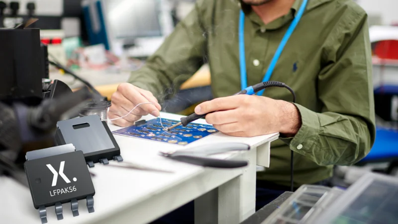
“We had to let customers know that this would do the same but better than the products they were using,” says Ding. “So, for the longest time, we kept that phrase in our marketing.” As the innovation gained traction though, engineers would gravitate towards LFPAK, looking for it by name, and Nexperia expanded the portfolio to offer increasing choice: the LFPAK56 (2002), LFPAK56E (2008), LFPAK33 (2010), LFPAK56D (2011), LFPAK88 (2019), with dual package versions and a total of 7 variants, housing over 400 products, now on the market.
Following the leader
The copying had started quite soon after it became clear that LFPAK wasn’t so much an alternative than a requirement. “Sure, by 2016, competitors were trying to ride the wave of LFPAK’s success,” says Adam Brown, “but it’s not an easy package to make. A continuous clip, external locking, top and bottom solder, interlocking mechanisms, this was an engineering masterpiece and competitors just didn’t have the expertise or experience to compete. Let’s just say that we had a big head start, being the inventors.”
An enduring legacy
With a design and construction optimized to provide the best thermal and electrical performance, cost and reliability, it’s no surprise LFPAK has been recognized as the de-facto standard power SO8 package.
With its size and weight advantages, LFPAK continues to enable industries to hone and refine their designs, specifically when weight and space is an issue.
The automotive industry is just one example. Even something as simple as a wing mirror now often incorporates a whole array of electronics, so size and weight of those components are a major design factor. So too is keeping the overall size and weight of the vehicle down in order to reduce emissions.
As the industry begins to evolve, LFPAK will be an enabler of many of the technologies around automated vehicles, such as double redundancy power steering systems, as well as the systems which power the next generation of EVs.
In addition to the automotive sector, LFPAK continues to enable greater miniaturisation across industries, as well as be a key driver towards more power efficient systems.
Success in numbers
Today around 90% of Nexperia’s MOSFET product range is LFPAK-based, with more than 400 devices across 7 distinct design variants. The company has shipped almost 10 billion LFPAK MOSFETs since production began, with 1.7 billion in 2021 alone—3,230 every minute, every day, round the clock to meet demand.
First MOSFETs, now bipolar transistors, and soon even more iterations of this profound innovation, Nexperia ships the LFPAK to 32 countries, 127 key customers and throughout its global distribution network.
Nexperia careers: Working on the next industry-changing technology.
Nexperia is a leading expert in the high-volume production of essential semiconductors, components that are required by every electronic design in the world. These products are recognized as benchmarks in efficiency - in process, size, power and performance - with industry-leading small packages that save valuable energy and space. Headquartered in Nijmegen, Netherlands, Nexperia annually ships more than 100 billion products. With decades of experience, supplying to the world’s biggest companies, Nexperia has over 14,000 employees across Asia, Europe and the U.S., offering global support.
We are a successful and ambitious international company with global reach and exciting plans for extraordinary growth. For that, we need exceptional people, and we hope that includes you.
So, join us and become an essential part of our energetic team, in a thriving global community of talented, multidisciplinary professionals. As a vital part of TeamNexperia, you will be working on meaningful technologies that touch every aspect of modern life.
Find out more: www.nexperia.com/careers