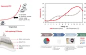
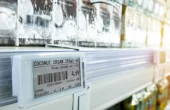
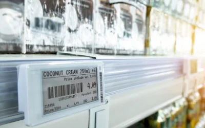
Wafer backgrinding is a crucial step in semiconductor manufacturing, as it prepares the wafer for further processing and packaging. The procedure comprises the thinning of silicon wafers by scraping out material from the backside, which is crucial for enhancing the functionality and dependability of semiconductor devices. This article examines the wafer backgrinding procedure, its difficulties, and the significance of quality control in ensuring the production of high-quality semiconductor devices.
Healthcare is undergoing a transformative shift with the rise of stick-to-skin wearable monitoring devices. These data-collecting marvels, such as continuous glucose or cardiac monitoring devices, offer convenience & real-time insights.This article explores capabilities, applications & market trends
Semiconductors are the building blocks of modern electronics, powering everything from smartphones to satellites. This in-depth guide provides a comprehensive understanding of semiconductors' engineering principles and applications, delving into their fundamental concepts, materials, devices, manufacturing processes, and their impact on today's technology landscape.
This article provides a technical overview of the brushless vs brushed motor paradigm, equipping design engineers with the analytical framework necessary to make informed, application-specific decisions.
Learn how USB 3.2 Gen 2x1 delivers 10Gbps high-speed performance with simpler single-lane routing, lower power consumption, and easier PCB design for embedded, FPGA, and industrial systems.
Explore how first-principles engineering and human judgment shape reliable high-voltage IC design, from yield thinking to long-term system lifetime and root-cause discipline.
This in depth article explores the theoretical foundation and practical considerations of connecting inductor in series for engineers and electronics students. Learn how series inductance works, why it increases total inductance, how mutual coupling affects it and how to design effective filters.
Learn how Altium Agile Teams enables secure hardware collaboration with centralized identity, role-based access, and full traceability — so teams can scale without sacrificing speed or control.
OMRONs XW4M/XW4N push-in terminal block PCB connectors are designed to simplify wiring, inspection, and maintenance while supporting consistent performance in industrial systems.
Soldering wires is the process of joining electrical conductors using a melted filler metal to create strong, low-resistance connections. This guide explains tools, techniques, heat control, materials, common defects, and engineering best practices for reliable electrical connections.
Wafer backgrinding is a crucial step in semiconductor manufacturing, as it prepares the wafer for further processing and packaging. The procedure comprises the thinning of silicon wafers by scraping out material from the backside, which is crucial for enhancing the functionality and dependability of semiconductor devices. This article examines the wafer backgrinding procedure, its difficulties, and the significance of quality control in ensuring the production of high-quality semiconductor devices.
Healthcare is undergoing a transformative shift with the rise of stick-to-skin wearable monitoring devices. These data-collecting marvels, such as continuous glucose or cardiac monitoring devices, offer convenience & real-time insights.This article explores capabilities, applications & market trends
In wearables, the design on paper often does not work in practice. In this world, your idea may only go as far as your chosen contract manufacturer can take you. It is the key role of the contract manufacturers to help you make the vital adjustment to make your product a success.
Additive electronics is intrinsically more sustainable than subtractive processes. Yet the current materials are often based on metallic inks and plastic substrates. This is a particular issue in medical wearables with disposable devices. Hence the need to develop sustainable material options
An In-depth Analysis of Features, Applications, and Selection Criteria for Embedded Systems Design. Discover the Advantages and Limitations of SPI, I2C, and UART for Efficient Data Exchange in Various Scenarios.
Integrated photonics, also known as planar lightwave circuits or integrated optical circuits, revolutionizes optical communication by leveraging the properties of light to process and transmit information. This cutting-edge technology offers superior efficiency and compactness compared to traditional electronic components, paving the way for faster and more energy-efficient communication systems. With its interdisciplinary nature encompassing materials science, quantum physics, and electrical engineering, integrated photonics presents an exciting and promising field of study and research in today's digital era.