Castellation PCB: A Comprehensive Guide to Design, Manufacturing, and Applications
Castellation PCB is a type of printed circuit board (PCB) that has a series of small, plated through holes along the edges of the board. These holes are used to create a connection between the board and other components in a circuit. This article delves into the design, manufacturing, and testing processes involved in creating castellation PCBs, providing insights into the key considerations and guidelines that engineers and manufacturers should follow to optimize their designs for performance, reliability, and manufacturability.

31 Jul, 2023. 21 minutes read
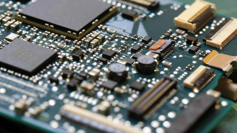
Close-up of the green kit circuit board.
Introduction
Castellation PCB is a type of printed circuit board that has become increasingly popular in recent years due to its unique design and benefits. This technology features plated-through holes (PTH) along the edges of the board, which create a connection between the board and other components in a circuit. The holes are typically small and closely spaced, allowing for a high density of connections in a small space. This makes Castellation PCBs ideal for applications where space is limited and a compact design is essential, such as in portable electronics and IoT devices.
Castellation PCBs have emerged as a popular choice for connecting and integrating electronic components in various applications, including consumer electronics, wearable devices, smart home systems, and gaming consoles. Their compact size, ease of assembly, and improved electrical performance make them an ideal solution for a wide range of applications. By understanding the intricacies of castellation PCBs, designers can create high-quality products that enhance the end-user experience and meet the demanding requirements of modern electronic devices.
One of the key benefits of Castellation PCB is its space-saving design. By using plated through holes (PTH) along the edges of the board, the overall size of the board can be reduced, which is essential in many applications. This also allows for a higher density of connections, which can be important in complex circuits. Another benefit of Castellation PCB is its versatility. It can be used in a wide range of applications, from simple circuits to more complex designs. It is also compatible with a variety of components, making it a popular choice for many engineers and designers.[1]
Castellation PCB Basics
What is a Castellation PCB?
A castellation PCB (Printed Circuit Board) is a type of PCB design that features small plated half-holes or notches along the edges of the board. These half-holes, also known as castellations, allow for easier board soldering and connection of the PCB to other panels or components. Castellation PCBs are commonly used in surface mount technology (SMT) applications, where components are mounted directly onto the surface of the board. This is one common approach to PCB assembly.
Castellation PCBs offer several advantages over traditional PCB designs. One of the main benefits is the ease of assembly, as the castellated holes provide a convenient board soldering point for connecting the board to other components or boards. This can lead to reduced assembly time and lower production costs.
Another advantage of castellation PCBs is their compact size. Because the castellated holes are located along the edge of the board, they do not take up valuable space on the PCB itself. This allows for a more compact design, which can be particularly beneficial in applications where space is limited, such as in wearable devices or Internet of Things (IoT) products.
In addition to these benefits, castellation PCBs also offer improved electrical performance. The castellated holes can serve as a direct electrical connection between the PCB and other components, reducing the need for additional connectors or wires. This can result in lower signal loss and improved signal integrity, especially in high-frequency applications.
However, there are also some challenges associated with castellation PCBs. One potential issue is the increased complexity of the manufacturing process. The creation of castellated holes requires precise drilling and plating techniques, which can increase production costs and lead times. Additionally, the small size of the castellated holes can make soldering more difficult, requiring skilled technicians and specialized equipment.
Despite these challenges, castellation PCBs continue to grow in popularity due to their numerous advantages and wide range of applications. From consumer electronics to medical devices, castellation PCBs offer a versatile and efficient solution for connecting and integrating electronic components.[2]
Further reading: Tented Via: The Ultimate Guide to PCB Design and Manufacturing Techniques
Castellation Types and Configurations
Full Castellations
Full castellations are a type of castellation where the entire edge of a printed circuit board (PCB) is notched, creating a series of protrusions that resemble the battlements of a castle. This design allows for easy soldering and electrical connection between two PCBs, as the castellations can be soldered directly to corresponding pads on the mating board. Full castellations are commonly used in applications where a PCB module or daughterboard needs to be securely connected to a main PCB, such as in wireless communication modules or sensor boards. PCB modules are commonly used in Castellation PCBs to provide additional functionality and features. A PCB module is a small circuit board that is designed to be integrated into a larger circuit board or system. These modules can be pre-built and tested, which helps to reduce the time and cost of developing a new circuit board.
Partial Castellations
Partial castellations, also known as half castellations, are similar to full castellations but feature notches only on a portion of the PCB edge. This configuration is typically used when only specific sections of the board require electrical connections, or when space constraints limit the use of full castellations. Partial castellations can be found in applications such as compact power supply modules or in situations where a PCB must be connected to a flexible circuit.
Staggered Castellations
Staggered castellations are a variation of the full or partial castellation design, where the notches are offset from one another along the edge of the PCB. This configuration can improve the mechanical stability of the connection between two boards, as the staggered pattern distributes the stress more evenly across the solder joints. Staggered castellations are often used in high-vibration environments or in applications where the PCB connection may be subject to mechanical stress, such as in automotive or aerospace electronics.
Castellation Configurations
In addition to the types of castellations, several common configurations can be employed to optimize the electrical and mechanical performance of the connection. These configurations include:
Single-row castellations: A single row of notches is created along the edge of the PCB. This configuration is the simplest and most common, suitable for a wide range of applications.
Double-row castellations: Two parallel rows of notches are created along the edge of the PCB, providing increased connection density and improved mechanical stability. Double-row castellations are often used in high-density interconnects or in situations where additional mechanical support is required.
Interleaved castellations: The notches in the castellations are arranged in an interleaved pattern, with each notch in one row offset from the notches in the adjacent row. This configuration can provide improved electrical performance by reducing crosstalk and signal interference between adjacent connections.
Each castellation type and configuration offers unique advantages and trade-offs, and the choice of which to use depends on the specific requirements of the application, such as the desired electrical performance, mechanical stability, and space constraints.[3]
Castellation PCB Design
Design Attributes
In castellation PCB design, there are certain features a designer must put into consideration. These specific characteristics or features are referred to as design attributes. In the context of circuit board design, design attributes might include things like the size and shape of the board, the number and type of components used, the power requirements, the communication interfaces, and the mechanical mounting options.
Other design attributes might include the cost of the board, the level of complexity, the level of reliability required, and the environmental conditions that the board will be exposed to. Designers need to carefully consider these attributes when designing a circuit board, as they can have a significant impact on the performance, cost, and overall quality of the board. Here are some considerations:
Castellation Size and Spacing
The size and spacing of the castellated holes play a crucial role in the electrical and mechanical performance of the PCB. Smaller castellations can allow for higher connection density but may be more challenging to manufacture and solder. Larger castellations can provide stronger mechanical connections but may occupy more space on the PCB. The spacing between castellations should be sufficient to prevent solder bridging and ensure reliable electrical connections. Typical castellation hole diameters range from 0.4 to 1.0 mm, with spacing between holes varying from 0.5 to 1.5 mm, depending on the application requirements.
Pad Design
The design of the pads on both the castellation PCB and the mating board is critical for ensuring a reliable solder joint. Pads should be large enough to accommodate the castellated holes and provide sufficient surface area for soldering. Non-solder mask defined (NSMD) pads, where the solder mask opening is larger than the copper pad, are often recommended for castellation PCBs, as they provide better solder joint strength and reliability.
Solder Mask and Silkscreen
The solder mask and silkscreen layers play an important role in the manufacturability and assembly of castellation PCBs. The solder mask should be carefully designed to prevent solder bridging between adjacent castellations, while still allowing for proper solder flow. The silkscreen layer should indicate the orientation and position of the castellation PCB, as well as any relevant component markings, to facilitate accurate assembly.
Thermal Management
Castellation PCBs, like any other PCB, must be designed with proper thermal management in mind. This is particularly important in high-power applications or when the PCB is used in a high-temperature environment. Techniques such as incorporating thermal vias, using thicker copper layers, or selecting materials with better thermal conductivity can help to dissipate heat more effectively and prevent thermal issues.
Design for Manufacturability (DFM)
Finally, it is essential to consider design for manufacturability (DFM) when creating a castellation PCB. This involves designing the PCB in such a way that it can be easily and cost-effectively manufactured, while still meeting the required performance and reliability specifications. DFM considerations for castellation PCBs may include selecting appropriate materials, optimizing the layout for efficient fabrication, and ensuring that the design adheres to the manufacturer's specific guidelines and capabilities.[4]
Design Rules and Guidelines
PCB Edge Clearance
One of the critical design rules for castellation PCBs is maintaining adequate edge clearance. Edge clearance refers to the distance between the castellated holes and the edge of the PCB. This clearance is essential to ensure the structural integrity of the board during manufacturing and assembly. A general guideline is to maintain a minimum edge clearance of 0.5 mm, although this value may vary depending on the specific requirements of the application and the manufacturing capabilities of the PCB supplier.
Castellation Hole Size and Spacing
The size and spacing of the castellated holes are crucial factors in determining the electrical performance and manufacturability of the PCB. The hole size should be large enough to accommodate the solder and provide a reliable electrical connection, but not so large that it compromises the structural integrity of the board. A typical castellation hole diameter ranges from 0.6 mm to 1.2 mm, depending on the application and manufacturing capabilities.
The spacing between castellated holes should be sufficient to prevent solder bridging and ensure proper electrical isolation between adjacent connections. A general guideline is to maintain a minimum spacing of 0.8 mm between castellated holes, although this value may vary depending on the specific requirements of the application and the manufacturing capabilities of the PCB supplier.
Plating Thickness
The thickness of the plating on the castellated holes is another critical design parameter. The plating thickness should be sufficient to provide a reliable electrical connection and withstand mechanical stress during assembly and operation. A typical plating thickness for castellation PCBs ranges from 20 µm to 30 µm, although this value may vary depending on the specific requirements of the application and the manufacturing capabilities of the PCB supplier.
Solder Mask and Silkscreen Considerations
Proper application of solder mask and silkscreen is essential for castellation PCBs. The solder mask should be designed to expose the castellated holes and their corresponding pads, allowing for easy soldering during assembly. Additionally, the silkscreen should be used to clearly label the castellated holes and their functions, ensuring proper orientation and connection during assembly.
Thermal Management
Castellation PCBs may require special considerations for thermal management, particularly in high-power or high-temperature applications. Proper thermal management can be achieved through the use of thermal vias, copper pours, or heat sinks, depending on the specific requirements of the application. Designers should carefully consider the thermal requirements of their castellation PCBs and incorporate appropriate thermal management strategies to ensure reliable operation and prevent thermal-related failures.
By following these design rules and guidelines, designers can create castellation PCBs that are both manufacturable and capable of meeting the electrical and mechanical requirements of their specific applications.
Design Software and Tools
Selecting the right design software and tools is crucial for creating a successful castellation PCB design. These tools can help streamline the design process, improve accuracy, and ensure that the final product meets the required specifications. Some popular design software and tools used for castellation PCB design include:
Altium Designer
Altium Designer is a powerful and versatile PCB design software that offers a wide range of features and capabilities, including support for castellation PCB design. With its advanced routing and layout tools, designers can easily create and optimize castellation patterns, manage pad designs, and ensure proper spacing between castellations. Altium Designer also includes built-in design rule checks (DRC) to help identify and correct potential issues before manufacturing.
Cadence Allegro
Cadence Allegro is another popular PCB design software that provides comprehensive support for castellation PCB design. Its advanced layout and routing tools allow designers to create precise castellation patterns and optimize pad designs for reliable solder joints. Allegro also offers robust DRC capabilities, ensuring that designs adhere to manufacturing guidelines and specifications.
KiCad
KiCad is an open-source PCB design software that offers a range of features and capabilities for castellation PCB design. With its user-friendly interface and extensive library of components, KiCad makes it easy for designers to create castellation patterns, manage pad designs, and ensure proper spacing between castellations. KiCad also includes built-in DRC functionality to help identify and correct potential design issues.
EAGLE
EAGLE, now part of Autodesk, is a widely used PCB design software that supports castellation PCB design. Its intuitive interface and powerful layout and routing tools enable designers to create accurate castellation patterns and optimize pad designs for reliable solder joints. EAGLE also offers built-in DRC capabilities to ensure that designs meet manufacturing guidelines and specifications.
These software tools are used to design breakout boards and other types of circuit boards. Breakout boards are another type of circuit board that is commonly used in conjunction with Castellation PCBs. A breakout board is a small PCB that is designed to "break out" a specific component or interface from a larger circuit board or system. These boards typically provide a simple interface, such as a set of pins or connectors, that can be easily connected to other components or devices.
Using the right design software and tools can significantly improve the efficiency and accuracy of the castellation PCB design process. By leveraging the advanced features and capabilities of these tools, designers can create high-quality castellation PCBs that meet the required performance and reliability specifications, while also ensuring manufacturability and cost-effectiveness.
Castellation PCB Manufacturing
Manufacturing Process
The manufacturing process of castellation PCBs involves several key steps, each of which must be carefully executed to ensure the quality and reliability of the final product. These steps include:
1. PCB Design and Layout: The first step in the manufacturing process is the creation of the PCB design and layout, which includes the placement of components, routing of traces, and the design of castellations. This stage is crucial for ensuring that the PCB meets the required electrical, mechanical, and thermal performance specifications.
2. Material Preparation: Once the design is finalized, the appropriate materials must be selected and prepared for the manufacturing process. This includes choosing the right substrate material, such as FR-4 or high-frequency laminates, and the suitable copper thickness for the application. The materials are then cut to size and prepared for the subsequent fabrication steps.
3. Drilling and Plating: The next step in the manufacturing process is drilling holes for the castellations. This requires precise drilling equipment and careful alignment to ensure that the holes are accurately positioned and have the correct dimensions. After drilling, the holes are plated with a thin layer of copper to create the electrical connection between the layers of the PCB.
4. Imaging and Etching: Following the drilling and plating process, the PCB is imaged with the desired circuit pattern using a photoresist material. This involves exposing the photoresist to ultraviolet light through a photomask, which transfers the circuit pattern onto the PCB. The exposed areas of the photoresist are then developed and removed, leaving the desired circuit pattern on the board. The exposed copper is then etched away, leaving only the circuit traces and castellations.
5. Solder Mask and Silkscreen Application: After etching, a solder mask is applied to the PCB to protect the copper traces and prevent solder bridging between adjacent castellations. The solder mask is typically applied using a screen printing or liquid photo imaging (LPI) process. Once the solder mask is cured, a silkscreen layer is added to the PCB to provide component markings and other relevant information.
6. Surface Finish: To ensure reliable soldering and electrical connections, a surface finish is applied to the exposed copper areas of the PCB, including the castellations. Common surface finishes for castellation PCBs include Electroless Nickel Immersion Gold (ENIG), Immersion Silver, and Hot Air Solder Leveling (HASL).
7. Quality Control and Testing: The final step in the manufacturing process is quality control and testing. This involves inspecting the PCB for any defects, such as misaligned castellations, solder mask issues, or etching errors. Electrical testing is also performed to ensure that the PCB meets the required performance specifications. This may include continuity testing, insulation resistance testing, and impedance testing.
By carefully executing each of these steps, manufacturers can produce high-quality castellation PCBs that meet the demanding requirements of modern electronic applications.[5]
Material Selection
Selecting the appropriate materials for a castellation PCB is crucial for ensuring the desired performance, reliability, and manufacturability of the final product. Several factors must be considered when choosing materials, including electrical properties, thermal performance, and mechanical stability. Some of the most common materials used in castellation PCBs are:
FR-4
FR-4 is the most widely used material for PCBs, including castellation PCBs. It is a composite material made from woven fiberglass cloth impregnated with epoxy resin. FR-4 offers a good balance of electrical, thermal, and mechanical properties, making it suitable for a wide range of applications. It has a relatively low cost and is readily available, which contributes to its popularity. However, FR-4 may not be suitable for high-frequency or high-temperature applications, as its electrical and thermal performance can degrade under these conditions.
High-Frequency Materials
For high-frequency applications, specialized materials with low dielectric loss and stable electrical properties are required. Some examples of high-frequency materials include the Rogers RO4000 series, the Taconic RF series, and the Isola I-Tera MT series. These materials are designed to minimize signal loss and maintain consistent performance at high frequencies, making them ideal for castellation PCBs used in RF and microwave applications. However, high-frequency materials are typically more expensive than standard FR-4 and may have more stringent manufacturing requirements.
High-Temperature Materials
In high-temperature applications, materials with excellent thermal stability and resistance to thermal degradation are essential. Some examples of high-temperature materials include polyimide, Rogers RO3000 series, and Isola IS410. These materials can withstand elevated temperatures without significant loss of electrical or mechanical performance, making them suitable for castellation PCBs used in harsh environments or high-power applications. However, high-temperature materials can be more difficult to process and may have higher costs compared to standard FR-4.
For applications requiring superior thermal management, metal-core PCBs (MCPCBs) can be an effective solution. MCPCBs consist of a metal base layer, typically aluminum or copper, which is laminated with a dielectric layer and a copper circuit layer. The metal base layer provides excellent heat dissipation, allowing for more efficient thermal management in high-power or high-temperature applications. Castellation PCBs can be designed with a metal core to improve thermal performance, but the manufacturing process for MCPCBs can be more complex and costly compared to traditional PCB materials.
When selecting materials for a castellation PCB, it is essential to consider the specific requirements of the application, such as the operating frequency, temperature range, and power levels. By choosing the appropriate materials, designers can optimize the performance, reliability, and manufacturability of their castellation PCBs.
Quality Control and Testing
Ensuring the quality and reliability of Castellation PCBs is crucial for their successful integration into electronic devices. Quality control measures and testing methods are implemented throughout the manufacturing process to identify and address potential issues before they become critical.
Visual Inspection
Visual inspection is a fundamental step in the quality control process for castellation PCBs. Skilled technicians or automated optical inspection (AOI) systems are used to examine the PCBs for any visible defects, such as misaligned castellations, solder bridges, or missing components. This inspection helps to identify and correct issues early in the manufacturing process, reducing the risk of costly rework or product failures.
Electrical Testing
Electrical testing is performed to ensure that the Castellation PCBs meet the required performance specifications and are free from any electrical defects. Common electrical tests include continuity testing, which verifies that all intended connections are present and functioning correctly, and isolation testing, which checks for any unintended short circuits between adjacent conductors. These tests can be performed using automated test equipment (ATE) or manual testing methods, depending on the complexity and volume of the PCBs being produced.
Solder Joint Integrity Testing
The integrity of the solder joints between the castellation PCB and the mating board is critical for ensuring reliable electrical connections and mechanical stability. Various testing methods can be employed to assess the quality of the solder joints, including X-ray inspection, which can reveal hidden defects such as voids or insufficient solder coverage, and shear testing, which measures the mechanical strength of the solder joint by applying a force perpendicular to the joint. These tests help to identify potential issues with the soldering process and ensure that the castellation PCBs are properly connected to their mating boards.
Environmental and Stress Testing
Castellation PCBs may be subjected to a variety of environmental and mechanical stresses during their lifetime, such as temperature fluctuations, humidity, vibration, or shock. To ensure that the PCBs can withstand these conditions and maintain their performance and reliability, they are often subjected to environmental and stress testing during the manufacturing process. Common tests include thermal cycling, which exposes the PCBs to repeated temperature changes to assess their resistance to thermal stress, and vibration testing, which simulates the mechanical stresses experienced during transportation or operation in high-vibration environments.
By implementing a comprehensive quality control and testing program, manufacturers can ensure that Castellation PCBs meet the required performance and reliability standards, reducing the risk of product failures and enhancing the overall quality of the electronic devices in which they are used.
Castellation PCB Applications
Consumer Electronics PCB
Consumer Electronics
Castellation PCBs play a significant role in the design and manufacturing of consumer electronics. Their compact size, ease of assembly, and improved electrical performance make them an ideal choice for various applications in this sector. Some examples of consumer electronics that utilize Castellation PCBs include:
Smartphones and Tablets
Modern smartphones and tablets require compact and efficient electronic components to fit within their slim form factors. Castellation PCBs are often used in these devices to connect various modules, such as wireless communication modules, power management modules, and sensor boards. The use of castellation PCBs in smartphones and tablets allows for a more streamlined assembly process and improved electrical performance, contributing to the overall user experience.
Wearable Devices
Wearable devices, such as smartwatches and fitness trackers, demand compact and lightweight electronic components that can fit within their small form factors. Castellation PCBs are an excellent choice for these applications, as they enable secure connections between various components while occupying minimal space. The use of castellation PCBs in wearable devices ensures reliable performance and extended battery life, which are critical factors for user satisfaction.
Bluetooth Devices
Castellation PCBs are often used in Bluetooth devices due to their space-saving design. Bluetooth devices require a compact design to be portable and easy to use, and Castellation PCBs help to achieve this by allowing for a high density of connections in a small space. Castellation PCBs also provide a secure and reliable connection between the Bluetooth device and other components in the circuit, which is essential for maintaining a strong signal. Overall, Castellation PCBs are a popular choice for Bluetooth devices due to their compatibility, versatility, and ability to create a compact design.
Smart Home Devices
Smart home devices, such as smart speakers, security cameras, and connected lighting systems, often require efficient and reliable electronic components to ensure seamless operation. Castellation PCBs are commonly used in these devices to connect various modules and components, such as sensors, microcontrollers, and wireless communication modules. The use of castellation PCBs in smart home devices contributes to improved performance, reliability, and ease of installation.
Gaming Consoles
Gaming consoles require high-performance electronic components to deliver an immersive gaming experience. Castellation PCBs are often used in these devices to connect various modules, such as graphics processing units (GPUs), central processing units (CPUs), and memory modules. The use of castellation PCBs in gaming consoles allows for efficient heat dissipation, improved signal integrity, and reduced assembly time, all of which contribute to the overall performance and user experience.
Further reading: TPU vs GPU in AI: A Comprehensive Guide to Their Roles and Impact on Artificial Intelligence
Inverter
Inverters are electronic devices that are used to convert DC power into AC power. They are commonly used in a variety of applications, including renewable energy systems, backup power systems, and motor control systems. Castellation PCBs can be used in the design and manufacture of inverters, and offer many advantages over other types of PCBs. One advantage of using castellation PCBs in inverters is that they are well-suited for high-power applications. Castellation PCBs are designed with small notches or cutouts along the edges, which allow them to be easily mounted onto other boards or systems. This makes them ideal for use in inverters, which often require high-power connections between different components.
Another advantage of using castellation PCBs in inverters is that they offer greater flexibility in the design and layout of the board. Castellation PCBs can be designed with a variety of shapes and sizes, which allows designers to create custom layouts that are optimized for their specific application. This can help to improve the performance and efficiency of the inverter, while also reducing the overall size and weight of the system.
By incorporating castellation PCBs into consumer electronics, manufacturers can achieve compact designs, streamlined assembly processes, and improved electrical performance, ultimately enhancing the end-user experience.
Industrial Automation
Role of Castellation PCBs in Industrial Automation
Castellation PCBs play a significant role in industrial automation, as they provide reliable and efficient connections between various electronic components and systems. Industrial automation involves the use of control systems, such as computers and robots, to operate and manage manufacturing processes and machinery. Castellation PCBs are often used in these control systems to facilitate communication between different devices and ensure seamless operation.
Examples of Castellation PCB Applications in Industrial Automation
One example of castellation PCB usage in industrial automation is in programmable logic controllers (PLCs). PLCs are widely used in manufacturing processes to control and monitor machinery, sensors, and actuators. Castellation PCBs can be employed in PLC modules to enable easy and secure connections between the main controller and various input/output (I/O) devices.
Another example is in the design of motor control systems. Castellation PCBs can be used to create compact and reliable connections between motor controllers and sensors, such as encoders or temperature sensors. This allows for precise control of motor speed, position, and torque, which is essential for maintaining the efficiency and accuracy of automated processes.
In addition, castellation PCBs can be found in industrial communication systems, such as Ethernet switches and gateways, which facilitate data exchange between different devices and systems within an industrial environment. The use of castellation PCBs in these communication systems ensures reliable and high-speed data transfer, which is critical for real-time monitoring and control of automated processes.
Advantages of Castellation PCBs in Industrial Automation
There are several advantages to using Castellation PCBs in industrial automation applications, including:
Reliability: The robust solder joints created by Castellation PCBs ensure reliable electrical connections, even in harsh industrial environments where vibration, temperature fluctuations, and electromagnetic interference may be present.
Compactness: The small size of castellation PCBs allows for more compact designs, which can be particularly beneficial in space-constrained industrial applications, such as robotic arms or conveyor systems.
Ease of Assembly: The castellated holes provide a convenient soldering point for connecting the PCB to other components or boards, reducing assembly time and lowering production costs.
Improved Electrical Performance: Castellation PCBs can offer better electrical performance compared to traditional PCB designs, as the castellated holes serve as a direct electrical connection between the PCB and other components, reducing the need for additional connectors or wires.
By incorporating castellation PCBs into industrial automation systems, designers can create more reliable, compact, and efficient solutions that meet the demanding requirements of modern manufacturing processes.
Internet of Things (IoT)
Role of Castellation PCBs in IoT Devices
Castellation PCBs play a significant role in the design and development of Internet of Things (IoT) devices. IoT devices often require compact, high-density electronic components to enable seamless communication and data processing. Castellation PCBs, with their small form factor and ease of assembly, are well-suited for IoT applications, as they allow for efficient integration of various electronic components, such as sensors, microcontrollers, and communication modules.
Examples of IoT Devices Using Castellation PCBs
Numerous IoT devices utilize castellation PCBs to achieve compact designs and reliable connections between components. Some examples include:
Smart home devices: Devices such as smart thermostats, lighting controls, and security systems often use castellation PCBs to connect various sensors and communication modules, enabling seamless integration with other smart devices and home automation systems.
Wearable devices: Wearable technology, such as fitness trackers and smartwatches, requires compact and lightweight electronic components. Castellation PCBs can be used to connect sensors, microcontrollers, and wireless communication modules in these devices, ensuring reliable performance and minimal space requirements.
Industrial IoT sensors: Industrial IoT applications often involve the deployment of numerous sensors to monitor and control various processes. Castellation PCBs can be used to connect these sensors to data processing and communication modules, enabling efficient data collection and analysis.
Benefits of Using Castellation PCBs in IoT Applications
There are several benefits to using Castellation PCBs in IoT applications, including:
Compact design: Castellation PCBs enable the creation of compact and lightweight electronic components, which is crucial for IoT devices with limited space and weight constraints.
Ease of assembly: The castellated holes on the PCBs facilitate easy soldering and connection of components, reducing assembly time and costs.
Improved electrical performance: Castellation PCBs can provide direct electrical connections between components, reducing the need for additional connectors or wires, which can result in lower signal loss and improved signal integrity.
Scalability: Castellation PCBs can be easily integrated into a wide range of IoT devices, making them versatile solutions for various applications and industries.
By leveraging the advantages of castellation PCBs, IoT device manufacturers can create compact, efficient, and reliable products that meet the growing demands of the IoT market.[6]
Conclusion
Castellation PCBs offer numerous advantages in various applications, including consumer electronics, wearable devices, smart home systems, and gaming consoles. Their compact size, ease of assembly, and improved electrical performance make them an ideal choice for connecting and integrating electronic components. By understanding the design, manufacturing, and testing processes involved in creating castellation PCBs, engineers and manufacturers can optimize their designs for performance, reliability, and manufacturability, ultimately enhancing the end-user experience.
Frequently Asked Questions (FAQs)
1. What is a castellation PCB?
A castellation PCB is a type of printed circuit board that features small plated half-holes or notches along the edges of the board. These half-holes, also known as castellations, allow for easier soldering and connection of the PCB to other boards or components.
2. What are the advantages of castellation PCBs?
Castellation PCBs offer several advantages, including ease of assembly, compact size, and improved electrical performance. They enable secure connections between various components while occupying minimal space, making them suitable for a wide range of applications.
3. What are the different types of castellations?
There are several types of castellations, including full castellations, partial castellations, and staggered castellations. Each type offers unique advantages and trade-offs, depending on the specific requirements of the application.
4. What are some common applications of castellation PCBs?
Castellation PCBs are commonly used in consumer electronics, wearable devices, smart home systems, and gaming consoles. Their compact size and ease of assembly make them an ideal choice for connecting and integrating electronic components in these applications.
5. What factors should be considered when designing a castellation PCB?
When designing a castellation PCB, several factors should be considered, including castellation size and spacing, pad design, solder mask and silkscreen application, thermal management, and design for manufacturability (DFM). These considerations help ensure optimal performance, manufacturability, and reliability of the final product.
References:
Venus Kohli (Wevolver), 2023. Castellated Holes: The Ultimate Guide to Their Advantages and Applications. Available at: https://www.wevolver.com/article/castellated-holes-the-ultimate-guide-to-their-advantages-and-applications (Accessed: July 20, 2023).
The Engineering Knowledge, 2023. How to Design a Castellated PCBs Board in 2023. Available at: https://www.theengineeringknowledge.com/castellated-pcb/ (Accessed: July 20, 2023).
Zachariah Peterson, 2021. How to Design Castellated Holes and Edges in a PCB for an SMD Module. Available at: https://resources.altium.com/p/how-design-castellated-holes-pcb-smd-module (Accessed: July 20, 2023).
Absolute Electronics, 2020. Castellated Holes: PCB Guide. Available at: https://absolutepcbassembly.com/castellated-holes-pcb/ (Accessed: July 20, 2023)
Sierra Circuits, 2023. How to Design Castellated Circuit Board in Altium Designer and Allegro. Available at: https://www.protoexpress.com/blog/how-to-design-castellated-circuit-board-in-altium-designer-and-allegro/#:~:text=Castellated%20pins%20are%20manufactured%20by,circuits%20to%20the%20main%20board. (Accessed: July 20, 2023)
WellPCB, 2023. Castellated PCB: An Excellent Way to Assemble Boards. Available at: https://www.wellpcb.com/castellated-pcb.html (Accessed: July 20, 2023).