Wafer Backgrinding: An In-Depth Guide to Semiconductor Manufacturing
Wafer backgrinding is a crucial step in semiconductor manufacturing, as it prepares the wafer for further processing and packaging. The procedure comprises the thinning of silicon wafers by scraping out material from the backside, which is crucial for enhancing the functionality and dependability of semiconductor devices. This article examines the wafer backgrinding procedure, its difficulties, and the significance of quality control in ensuring the production of high-quality semiconductor devices.

11 Jul, 2023. 22 minutes read
Silicon Wafer in Die Attach Machine
Introduction
The semiconductor manufacturing process involves the creation of intricate electronic circuits on silicon wafers. These wafers serve as the foundation for the fabrication of integrated circuits (ICs) and other electronic components. As the demand for smaller, faster, and more energy-efficient devices increases, the need for thinner wafers becomes more essential. Wafer backgrinding, also known as wafer thinning, plays a vital role in achieving this goal by regulating wafer thickness, which is necessary to manufacture ultra-thin wafers that are used to produce well-proportioned and high-density packaging in compact electronic devices.
After backgrinding, the wafer is further processed through dicing to create transistors, diodes, and other components that are integrated into semiconductor chips. Many people often mistake wafer dicing for wafer backgrinding. While wafer backgrinding and wafer dicing are both important processes in the manufacturing of semiconductor devices, they are not the same. After a wafer has been thinned through backgrinding, it is cut into individual chips using a dicing saw. The dicing saw uses a high-speed blade to cut through the wafer, creating individual chips that can be further processed and assembled into complete semiconductor devices. The dicing process is critical to ensure that the chips are cut accurately and without damage, which can affect their performance and reliability.
Therefore, both wafer backgrinding and dicing are important steps in the manufacturing of high-quality semiconductor chips and are both considered front-end processes in semiconductor manufacturing. The front-end processes are followed by back-end processes, which involve assembling, packaging, and testing individual chips. Even after the chips have already been placed on the wafer, any error during processing will reduce manufacturing yield and raise costs. As a result, obtaining the proper wafer thickness before assembly is crucial in the production of semiconductors. Therefore, while wafer backgrinding is a front-end process, it is a critical step that enables the back-end processing of semiconductor device manufacturing.
Overview of Semiconductor Manufacturing
Semiconductor manufacturing is a complex process that involves the production of electronic devices, such as integrated circuits (ICs), by using semiconductor materials like silicon. The first step in the procedure is the production of a silicon wafer, which acts as the base for the electronic parts. To construct the necessary circuit patterns on the wafer, a series of fabrication operations, including photolithography, etching, and deposition, are performed. After the circuits have been created, the wafer is divided into individual chips, which are then packaged and tested before being used in various electronic devices. Role of Wafers in Manufacturing
Wafers are the foundation of semiconductor manufacturing. They are thin, flat discs made from high-purity single-crystal silicon, which provides the necessary electrical properties for electronic devices. Wafers serve as the substrate on which the electronic components are built, and their quality directly impacts the performance and reliability of the final product. The size of wafers has increased over the years, with the current standard being 300mm in diameter. Larger wafers allow for more chips to be produced per wafer, leading to increased efficiency and lower production costs.
Importance of Wafer Backgrinding
The wafer backgrinding or wafer thinning process is a critical step in semiconductor manufacturing, as it reduces the wafer's thickness to improve the final device's performance and form factor. Thinner wafers allow for smaller, lighter, and more power-efficient devices, which are essential for applications such as smartphones, wearables, and other portable electronics. One of the primary methods for wafer thinning is backgrinding, which involves mechanically grinding the backside of the wafer to achieve the desired thickness which is measured in microns. A micron (also written as µm or um) is a unit of measurement used to describe the thickness of the wafer after grinding. The use of microns as a unit of measurement is common in the semiconductor industry, as it allows for precise control over the thickness of wafers and the resulting chips. By carefully controlling the thickness of the wafer during backgrinding, semiconductor manufacturers can ensure that the chips produced from the wafer meet the required specifications for their intended use.
Backgrinding is a sensitive procedure because it must remove a sizeable amount of material without destroying the delicate circuitry on the front side of the wafer. To guarantee the quality and functionality of the finished product, the backgrinding process must be properly controlled. The right grinding wheel selection, grinding parameters, and quality control are all important factors in getting the desired outcomes.[1]
Recommended reading: Silicon Wafers: Everything You Need to Know
Wafer Backgrinding Process
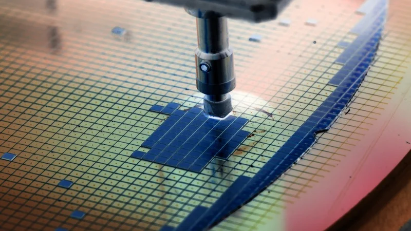
Wafer backgrinding process involves several steps, including wafer mounting, grinding wheel selection, and optimization of grinding parameters. Specialized equipment, such as backgrinding machines and metrology tools, are used to ensure precision and accuracy throughout the process. The processes are explained below:
Wafer Mounting
Wafer mounting is the first step in the backgrinding process, and it entails attaching semiconductor wafers to a carrier substrate, such as a plastic or metal ring, in preparation for wafer processing. The carrier substrate provides temporary mechanical support to the wafer and helps to prevent it from breaking or warping during wafer processing. The wafer mounting process typically involves applying a layer of adhesive or backgrinding tape to the backside of the wafer and then attaching it to the carrier substrate. The wafer and carrier substrates are then loaded into wafer processing equipment, such as a backgrinding or dicing saw, for further processing. The choice of mounting method is influenced by the wafer's size, thickness, and material qualities, among other things. Wafer mounting is a critical step in semiconductor manufacturing, as it helps to ensure that the wafer is held securely during processing and that the resulting chips are of high quality and reliability.
There are two primary types of wafer mounting techniques: adhesive mounting and wax mounting. Adhesive mounting involves the use of a thin layer of adhesive film, typically made of UV-curable or heat-sensitive materials, to attach the wafer to a support substrate, an example is lamination. Lamination refers specifically to the process of attaching a temporary carrier substrate to the backside of the wafer using an adhesive material. So while lamination is one specific type of adhesive mounting, not all adhesive mounting is lamination. Adhesive mounting offers several advantages, including easy removal of the wafer after grinding, minimal residue, and compatibility with various wafer materials. However, adhesive mounting may not be suitable for extremely thin wafers, as the adhesive film may not provide sufficient support during the grinding process.
On the other hand, wax mounting uses a layer of wax to bond the wafer to the support substrate. This approach can endure greater grinding forces and offers excellent support for thin wafers. Wax mounting does, however, come with several disadvantages, such as the necessity for additional cleaning procedures to remove wax residue and potential compatibility concerns with certain wafer materials.
The choice of mounting technique is determined by the wafer's unique needs and the intended backgrinding result. When choosing the best mounting technique, take into account elements such as wafer size, thickness, material qualities, and the desired thickness after grinding.
Grinding Wheel Selection
Selecting the right grinding wheel is crucial for achieving the desired wafer thickness and surface quality during the backgrinding process. The grinding wheel plays a significant role in determining the rate of material removal, surface roughness, and the risk of damage to the wafer. Various factors influence the choice of grinding wheel, including the type of abrasive material, grinding wheel bond, and grit size.
Types of Abrasive Materials
Grinding wheels are made from different abrasive materials, each with its characteristics and suitability for specific applications. In wafer backgrinding, the abrasive material used to thing the wafer is typically made of a conductive material, such as
Silicon carbide (SiC): Known for its hardness and sharpness, SiC is a popular choice for grinding silicon wafers. It offers a high material removal rate and an excellent surface finish.
Diamond: Diamond is the hardest known material and provides superior grinding performance, especially for hard and brittle materials like silicon. Diamond grinding wheels are often used for ultra-thin wafer grinding and applications that require high precision.
The conductive nature of the abrasive material helps to dissipate heat generated during the grinding process and to prevent static buildup, which could cause damage to the wafer. The wafer is typically mounted on a carrier substrate, which is conductive and helps ground the wafer during grinding. The conductive nature of the abrasive material and the carrier substrate are important factors in ensuring that the wafer is thinned to the desired thickness without damage or defects.
Grinding Wheel Bond
The bond is the material that holds the abrasive grains together in the grinding wheel. It plays a crucial role in determining the wheel's performance, wear rate, and quality of the ground surface. Common types of bonds used in wafer backgrinding include:
Resin bond: Resin-bonded wheels are known for their flexibility and ability to produce a smooth surface finish. They are widely used in wafer backgrinding due to their lower risk of causing wafer breakage and subsurface damage.
Vitrified bond: Vitrified-bonded wheels offer higher strength and rigidity compared to resin-bonded wheels. They are less prone to wear and provide more consistent grinding performance. However, they may be more likely to cause wafer breakage due to their rigidity.
Grit Size
The size of the abrasive grains in the grinding wheel is referred to as the grit size. It has a direct impact on the wafer's surface quality and rate of material removal. A coarser grit size results in a higher material removal rate but may produce a rougher surface finish. A coarser grit size, on the other hand, offers a smoother surface quality but can necessitate more grinding passes to achieve the necessary wafer thickness. The backgrinding process has various parameters, including the intended thickness and surface quality, and these dictate the grit size that should be used. In summary, choosing the right grinding wheel is crucial for obtaining the necessary wafer thickness and surface quality during wafer backgrinding. To achieve the best grinding performance and the lowest possible risk of wafer damage, factors such as the abrasive material, bond type, and grit size mentioned above, must be carefully taken into account.
Grinding Parameters
The grinding parameters play a crucial role in the wafer backgrinding process, as they directly impact the quality and performance of the final device. These parameters include grinding wheel speed, wafer rotation speed, grinding depth, and coolant flow rate. Proper control and optimization of these parameters are essential to ensure a smooth and uniform wafer surface while minimizing the risk of damage.
Grinding Wheel Speed
The grinding wheel speed refers to the rotational speed of the grinding wheel, typically measured in revolutions per minute (RPM). The optimal grinding wheel speed depends on factors such as the type of grinding wheel, the material being ground, and the desired surface finish. Higher grinding wheel speeds can result in faster material removal rates but may also increase the risk of surface damage and subsurface defects. Therefore, it is essential to find a balance between speed and quality to achieve the best results.
Wafer Rotation Speed
The wafer rotation speed is the speed at which the wafer rotates during the backgrinding process. Similar to the grinding wheel speed, the wafer rotation speed can impact the material removal rate and the quality of the final surface. A higher wafer rotation speed can lead to faster grinding but may also increase the risk of wafer breakage and surface damage. Careful control of the wafer rotation speed is necessary to ensure a consistent and uniform wafer thickness.
Grinding Depth
Grinding depth refers to the amount of material removed from the wafer during each pass of the grinding wheel. The grinding depth must be carefully controlled to achieve the desired wafer thickness while minimizing the risk of damage to the wafer. A smaller grinding depth can result in a smoother surface finish, but it may require more passes to achieve the desired thickness, increasing the overall processing time. Conversely, a larger grinding depth can reduce processing time but may increase the risk of surface and subsurface damage.
Coolant Flow Rate
The coolant flow rate is the rate at which the coolant is applied to the grinding area during the backgrinding process. The coolant assists to disperse heat produced during the grinding operation, lubricates the grinding interface, and reduces friction. To avoid overheating, which can harm the wafer thermally and impair device performance, an appropriate coolant flow rate is necessary. The ideal coolant flow rate is influenced by things including the type of grinding wheel, the type of wafer, and the grinding parameters. To achieve the best results, it is essential to keep the coolant flow rate constant throughout the backgrinding procedure.[2]
Challenges in Wafer Backgrinding
Wafer backgrinding is a delicate and complex process that requires precise control to achieve the desired results. Several challenges can arise during the backgrinding process, which can impact wafer quality and the performance of the final device. These challenges include wafer breakage, surface damage, and subsurface damage. Addressing these challenges is crucial for ensuring the production of high-quality semiconductor devices.
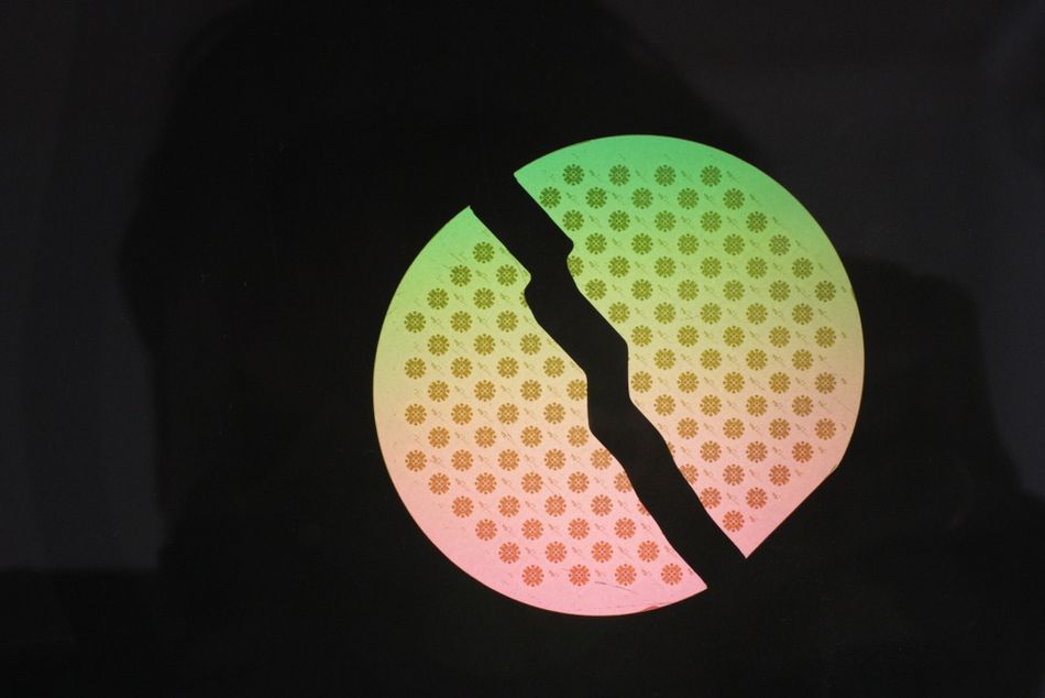
Wafer Breakage
Wafer breakage is a significant concern during the backgrinding process, as it can lead to material loss and increased production costs. The primary cause of wafer breakage is excessive stress applied to the wafer during grinding. This stress can result from various factors, such as improper mounting, uneven grinding wheel wear, or incorrect grinding parameters.
Wafer breakage can have serious consequences because it not only results in material loss but also ruins the production line and raises production expenses. Different strategies can be used to reduce wafer breakage. These include:
Proper wafer mounting: Ensuring the wafer is securely and uniformly mounted on the grinding chuck can help reduce stress and prevent breakage. Appropriate backgrinding tapes and mounting techniques are essential for achieving a secure and uniform mount.
Grinding wheel maintenance: Regular inspection and dressing of the grinding wheel can help maintain its shape and ensure even wear. This can help reduce stress on the wafer and minimize the risk of breakage.
Optimizing grinding parameters: Adjusting grinding parameters, such as wheel speed, feed rate, and grinding depth, can help control the stress applied to the wafer. By optimizing these parameters, the risk of wafer breakage can be significantly reduced.
Implementing these strategies can help minimize wafer breakage and ensure the production of high-quality semiconductor devices.[3]
Surface Damage
Surface damage is a common challenge encountered during the wafer backgrinding process. It refers to the defects and imperfections that can occur on the wafer surface as a result of the grinding process. These defects can include scratches, cracks, and pits, which can negatively impact the performance and reliability of the semiconductor devices fabricated on the wafer.
Surface damage during backgrinding can be caused by many sources. These consist of wafer mounting quality, grinding wheel selection, and grinding settings. For instance, using a grinding wheel with the wrong grit size or abrasive substance might result in excessive material removal and surface damage. Similarly, improper grinding parameters, such as excessive grinding force or speed, can cause the wafer to overheat and generate thermal stress, leading to surface defects.
To minimize surface damage during wafer backgrinding, it is essential to carefully select the appropriate grinding wheel and optimize the grinding parameters. This may involve using a grinding wheel with a suitable abrasive material and grit size, as well as adjusting the grinding force, speed, and coolant flow to maintain optimal grinding conditions. Additionally, proper wafer mounting can help to ensure that the wafer remains stable and well-supported during the grinding process, reducing the risk of surface damage.
Another approach to reducing surface damage is to employ post-grinding treatments, such as chemical mechanical polishing (CMP) or plasma etching. These processes can help to remove surface defects and improve the overall quality of the wafer surface. However, these additional steps can also increase the complexity and cost of the wafer manufacturing process, so it is essential to carefully consider the trade-offs when deciding on the best approach for a specific application.[4]
Subsurface Damage
Subsurface damage refers to the microscopic defects and structural changes that occur beneath the surface of the wafer during the backgrinding process. These defects can include microcracks, dislocations, and residual stress, which can negatively impact the performance and reliability of the semiconductor devices. Understanding the causes of subsurface damage and implementing techniques to minimize it is crucial for ensuring the quality of the final product.
One of the primary causes of subsurface damage is the mechanical stress induced by the grinding process. The grinding wheel's abrasive particles can generate high localized pressures on the wafer surface, forming microcracks and other defects. Additionally, the heat generated during grinding can cause thermal stress, which can further contribute to subsurface damage.
When grinding wafers, it's crucial to minimize subsurface damage. One way to achieve this is by selecting a grinding wheel with finer abrasive particles. This can reduce the mechanical stress applied to the wafer surface and limit damage. However, this approach may increase grinding time and reduce material removal rate, so it's important to strike a balance between damage reduction and process efficiency.
Another approach to reducing subsurface damage is optimizing the grinding parameters, such as the grinding speed, feed rate, and coolant flow. Adjusting these parameters can help control the amount of heat generated during grinding and reduce the mechanical stress on the wafer. For example, increasing the coolant flow can help dissipate heat more effectively, while reducing the grinding speed can lower the mechanical stress on the wafer surface.
Finally, post-grinding processes, such as chemical-mechanical polishing (CMP) or etching, can be used to remove a thin layer of material from the wafer surface, effectively eliminating any subsurface damage caused by the backgrinding process. These additional steps can help ensure the quality and performance of the final semiconductor devices.[5]
Wafer Backgrinding Quality Control
Quality control is an essential aspect of the wafer backgrinding process, as it ensures the production of high-quality semiconductor devices. Various quality control methods are employed to monitor and maintain the quality of the ground wafer surface, including surface roughness measurement, thickness uniformity measurement, and defect inspection. Metrology tools and techniques are critical for achieving accurate and reliable quality control measurements.
Surface Roughness Measurement
Surface roughness is an important parameter in wafer backgrinding, as it directly impacts the performance and reliability of the final device. Measuring surface roughness ensures that the ground wafer surface meets the required specifications and quality standards. Several methods can be used to measure surface roughness, each with its advantages and disadvantages.
Contact profilometry: Contact profilometry involves the use of a stylus that is dragged across the wafer surface to measure its roughness. This method provides high-resolution measurements and can detect small surface features. However, contact profilometry can be slow and may cause damage to the wafer surface due to the physical contact between the stylus and the wafer.
Optical profilometry: Optical profilometry is a non-contact method that uses light to measure the surface roughness of the wafer. This technique offers several advantages, including faster measurement times and no risk of surface damage. However, optical profilometry may be less accurate than contact profilometry for certain surface features and may be affected by the optical properties of the wafer material.
Atomic force microscopy (AFM): AFM is a high-resolution, non-contact method that uses a sharp probe to scan the wafer surface and measure its roughness. AFM provides extremely accurate measurements and can detect nanoscale surface features. However, AFM is slow and has a limited measurement area, making it less suitable for large-scale quality control applications.
The choice of surface roughness measurement method depends on factors such as the required accuracy, measurement speed, and potential risk of surface damage. By employing appropriate measurement techniques, manufacturers can ensure that the ground wafer surface meets the necessary quality standards and specifications.[6]
Thickness Uniformity Measurement
Thickness uniformity is a critical aspect of wafer quality, as it directly impacts the performance and reliability of the semiconductor devices fabricated on the wafer. Achieving a consistent and uniform wafer thickness is essential for ensuring optimal device performance and minimizing the risk of defects during subsequent processing steps. Therefore, measuring and maintaining thickness uniformity is a crucial aspect of the wafer backgrinding process.
There are several methods available for measuring wafer thickness uniformity, each with its advantages and disadvantages. Some of the most common methods include:
Optical methods: Optical techniques, such as interferometry and ellipsometry, can provide non-contact and non-destructive measurements of wafer thickness and uniformity. Interferometry uses the interference of light waves to measure the thickness of the wafer, while ellipsometry measures the change in polarization of light reflected from the wafer surface. Both methods offer high precision and accuracy, but they may be sensitive to surface roughness and require sophisticated equipment and expertise.
Mechanical methods: Mechanical techniques, such as contact profilometry and stylus profilometry, involve the use of a probe to physically measure the wafer's surface profile. Contact profilometry uses a diamond-tipped stylus that is dragged across the wafer surface, while stylus profilometry uses a stylus that is moved vertically to measure the wafer's thickness at different points. These methods can provide accurate and reliable measurements, but they may be slower and more prone to damage the wafer surface compared to optical methods.
Acoustic methods: Acoustic techniques, such as ultrasonic thickness measurement, use sound waves to measure the thickness of the wafer. An ultrasonic transducer sends a sound wave through the wafer, and the time it takes for the wave to travel through the material and reflect is used to calculate the thickness. Acoustic methods offer non-contact and non-destructive measurements, but they may be less accurate than optical or mechanical methods and can be affected by variations in material properties.
Each of these methods has its advantages and disadvantages, and the choice of the most suitable method depends on factors such as the required accuracy, measurement speed, and the specific characteristics of the wafer material. By carefully selecting the appropriate thickness uniformity measurement method and maintaining strict quality control during the backgrinding process, it is possible to achieve a high level of thickness uniformity and ensure the production of high-quality semiconductor devices.[7]
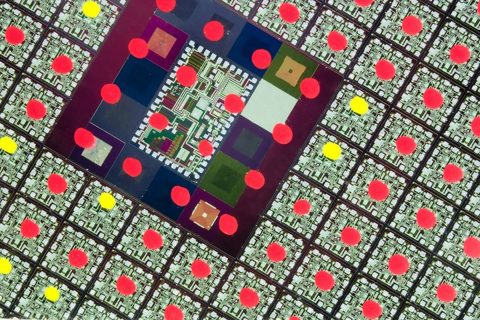
Defect Inspection
Defect inspection is an essential aspect of quality control in wafer backgrinding, as it helps to identify and quantify surface and subsurface defects that may impact the performance and reliability of the final semiconductor devices. Various inspection methods can be employed to detect and characterize defects, each with its advantages and disadvantages.
Optical Inspection
Optical inspection techniques use light to examine the wafer surface for defects, such as scratches, pits, and cracks. These methods include bright-field and dark-field microscopy, as well as laser scanning confocal microscopy. Optical inspection techniques are non-destructive and can provide high-resolution images of the wafer surface. However, they may have difficulty detecting subsurface defects or defects that are smaller than the wavelength of light used for inspection.
Scanning Electron Microscopy (SEM)
Scanning electron microscopy (SEM) uses a focused beam of electrons to generate high-resolution images of the wafer surface. SEM can detect surface defects with greater resolution than optical techniques and can also provide information about the chemical composition of the defects. However, SEM is a destructive inspection method, as it requires a small portion of the wafer to be removed for analysis. Additionally, SEM is typically slower and more expensive than optical inspection techniques.
Atomic Force Microscopy (AFM)
Atomic force microscopy (AFM) is a high-resolution imaging technique that uses a sharp probe to scan the wafer surface and measure the forces between the probe and the surface. AFM can detect surface defects with nanometer-scale resolution and can also provide information about surface roughness and topography. However, AFM is a slow inspection method, as it requires the probe to be scanned across the entire wafer surface, making it less suitable for high-throughput applications.
Recommended reading: Atomic Force Microscopy Explained: Principles, Construction, Working, and Applications
In summary, defect inspection is a critical aspect of wafer backgrinding quality control, as it helps to identify and quantify defects that may impact the performance and reliability of the final semiconductor devices. The choice of inspection method depends on factors such as the type of defects to be detected, the required resolution, and the throughput requirements of the manufacturing process. By employing appropriate inspection techniques, manufacturers can ensure the production of high-quality semiconductor devices with minimal defects.
Emerging Technologies in Wafer Backgrinding
As the demand for thinner and more efficient semiconductor devices continues to grow, new technologies and techniques are being developed to improve the wafer backgrinding process. These emerging technologies aim to address the challenges associated with traditional backgrinding methods, such as surface and subsurface damage, wafer breakage, and thickness uniformity. Some of the most promising emerging technologies in wafer backgrinding include:
Ultra-Precision Grinding
Ultra-precision grinding is an advanced grinding technique that uses ultra-fine abrasive particles and specialized grinding machines to achieve nanometer-scale surface finishes and thickness tolerances. This technology enables the production of ultra-thin wafers with minimal surface and subsurface damage, making it particularly suitable for applications in advanced semiconductor devices, such as 3D integrated circuits and flexible electronics. Ultra-precision grinding can also reduce the need for post-grinding processes, such as chemical-mechanical polishing, resulting in a more efficient and cost-effective manufacturing process.
Stress-Relief Grinding
Stress-relief grinding is a technique designed to minimize the mechanical stress induced during the backgrinding process. This method involves the use of specialized grinding wheels and process parameters that reduce the grinding forces and heat generation, thereby minimizing the risk of surface and subsurface damage. Stress-relief grinding can help improve the quality and reliability of semiconductor devices by reducing the occurrence of defects, such as microcracks and dislocations, which can impact device performance.
In-Situ Metrology and Process Control
In-situ metrology and process control technologies enable real-time monitoring and control of the wafer backgrinding process. These technologies use advanced sensors and control algorithms to measure critical process parameters, such as grinding force, temperature, and wafer thickness, and adjust the grinding parameters accordingly. By providing real-time feedback and control, in-situ metrology and process control technologies can help improve the consistency and quality of the backgrinding process, resulting in better device performance and yield.
Plasma-Assisted Grinding
Plasma-assisted grinding is an emerging technology that combines traditional grinding techniques with plasma processing to achieve improved wafer surface quality and reduced subsurface damage. In this method, plasma is generated at the grinding interface, which can modify the wafer surface properties and enhance the material removal process. Plasma-assisted grinding has the potential to reduce surface roughness, minimize subsurface damage, and improve the overall quality of the ground wafer.
In conclusion, emerging technologies in wafer backgrinding are paving the way for the production of thinner and more efficient semiconductor devices. By addressing the challenges associated with traditional backgrinding methods, these new technologies have the potential to revolutionize the semiconductor manufacturing process and enable the development of advanced electronic devices with improved performance and reliability.[8]
Conclusion
Wafer backgrinding is a critical step in semiconductor manufacturing, as it enables the production of thinner and more efficient electronic devices. The process involves several key aspects, including wafer mounting, grinding wheel selection, optimization of grinding parameters, and quality control. Addressing the challenges associated with wafer breakage, surface damage, and subsurface damage is essential for ensuring the production of high-quality semiconductor devices. By employing appropriate techniques and maintaining strict quality control, manufacturers can achieve the desired wafer thickness and surface quality while minimizing the risk of defects.
Frequently Asked Questions (FAQs)
1. What is the purpose of wafer backgrinding?
Wafer backgrinding is used to thin silicon wafers to the desired thickness, enabling the production of smaller and more efficient electronic devices. Thinner wafers allow for smaller, lighter, and more power-efficient devices, which are essential for applications such as smartphones, wearables, and other portable electronics.
2. What factors influence the choice of grinding wheel for wafer backgrinding?
The choice of a grinding wheel depends on factors such as the type of abrasive material, the wheel's bond, and its grit size. Common abrasive materials include silicon carbide and diamond, while bond types include resin and vitrified bonds. The grit size affects the rate of material removal and the surface finish of the wafer.
3. How is wafer thickness uniformity measured?
Wafer thickness uniformity can be measured using various methods, such as optical methods (interferometry and ellipsometry), mechanical methods (contact profilometry and stylus profilometry), and acoustic methods (ultrasonic thickness measurement). Each method has its advantages and disadvantages, and the choice depends on factors such as the required accuracy, measurement speed, and the specific characteristics of the wafer material.
4. What are some strategies to minimize wafer breakage during backgrinding?
To minimize wafer breakage, several strategies can be employed, such as proper wafer mounting, grinding wheel maintenance, and optimizing grinding parameters. Ensuring the wafer is securely and uniformly mounted on the grinding chuck can help reduce stress and prevent breakage. Regular inspection and dressing of the grinding wheel can help maintain its shape and ensure even wear. Adjusting grinding parameters, such as wheel speed, feed rate, and grinding depth, can help control the stress applied to the wafer.
5. How can surface and subsurface damage be minimized during wafer backgrinding?
To minimize surface and subsurface damage, it is essential to carefully select the appropriate grinding wheel and optimize the grinding parameters. This may involve using a grinding wheel with a suitable abrasive material and grit size, as well as adjusting the grinding force, speed, and coolant flow to maintain optimal grinding conditions. Additionally, post-grinding processes, such as chemical-mechanical polishing (CMP) or etching, can be used to remove surface defects and improve the overall quality of the wafer surface.
References
Muhammed Khan (Wevolver), 2023. How are Semiconductors Made? A Comprehensive Guide to Semiconductor Manufacturing. Available at: https://www.wevolver.com/article/how-are-semiconductors-made-a-comprehensive-guide-to-semiconductor-manufacturing (Accessed: July 6, 2023).
Köhler, J. (2014). Grinding Parameters. In: Laperrière, L., Reinhart, G. (eds) CIRP Encyclopedia of Production Engineering. Springer, Berlin, Heidelberg. https://doi.org/10.1007/978-3-642-20617-7_6424
Wafer World, 2021. Top Causes of Silicon Wafer Breakage. Available at: https://www.waferworld.com/post/top-causes-of-silicon-wafer-breakage (Accessed: July 6, 2023).
D. Echizenya and K. Sasaki, "Effect of surface damage on strength of silicon wafer for solar cells," 2014 International Conference on Electronics Packaging (ICEP), Toyama, Japan, 2014, pp. 14-18, doi: 10.1109/ICEP.2014.6826653.
Yin, Jf., Bai, Q. & Zhang, B. Methods for Detection of Subsurface Damage: A Review. Chin. J. Mech. Eng. 31, 41 (2018). https://doi.org/10.1186/s10033-018-0229-2
Keiichiro Mori et al 2020 Jpn. J. Appl. Phys. 59 SMMB06 DOI 10.35848/1347-4065/ab918c Available at: https://iopscience.iop.org/article/10.35848/1347-4065/ab918c
Maksym Myronov et al 2022 Semicond. Sci. Technol. 37 065003. DOI 10.1088/1361-6641/ac5f69 Available at: https://iopscience.iop.org/article/10.1088/1361-6641/ac5f69
KBV Research, 2022. Global Wafer Backgrinding Tape Market Size, Share & Industry Trends Analysis Report By Type (Non-UV and UV-Curable), By Wafer Size (12-Inch, 8-Inch, 6-Inch, and Others), By Regional Outlook, Strategy, Challenges and Forecast, 2021 - 2027. Available at: https://www.kbvresearch.com/wafer-backgrinding-tape-market/ (Accessed: July 7, 2023).