Featured
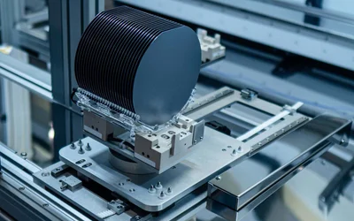
The semiconductor manufacturing field employs a range of etching techniques to craft intricate patterns and structures on material surfaces, with dry etching and wet etching being primary methods.
The semiconductor manufacturing field employs a range of etching techniques to craft intricate patterns and structures on material surfaces, with dry etching and wet etching being primary methods.
PCB Trace Width Calculator
Glossary of Semiconductors Terms
The semiconductor manufacturing field employs a range of etching techniques to craft intricate patterns and structures on material surfaces, with dry etching and wet etching being primary methods.
According to leading trade publication, Enterprise IoT Insights, more than 80 percent of OEMs in the asset tracking space are releasing products for cellular IoT low power wide area networks (LPWANs). Also, LTE-M trackers have high growth as mobile operators roll out LTE-M networks.
Despite specific industries experiencing slowdowns caused by the Covid-19 pandemic, projections in the Bluetooth technology market are optimistic through the remainder of 2021 and beyond.
Semiconductors are the building blocks of modern electronics, powering everything from smartphones to satellites. This in-depth guide provides a comprehensive understanding of semiconductors' engineering principles and applications, delving into their fundamental concepts, materials, devices, manufacturing processes, and their impact on today's technology landscape.
13 minutes read.
20 minutes read.
16 minutes read.
20 minutes read.
20 minutes read.
13 minutes read.


Semiconductors
Nordic Semiconductor is a fabless semiconductor company specializing in wireless technology that powers the IoT.
181 Posts
A guide covering the full radio-frequency design workflow, starting from setting specifications and choosing topologies to matching, simulation, layout, and verification, to help antenna engineers.
This article presents a detailed technical exploration of SiC MOSFET devices, covering material physics, device structure, switching behavior, and practical design considerations for high-efficiency power electronics systems.
This article is a comprehensive technical guide to relay wiring diagrams, covering 4-pin and 5-pin configurations, working principles, safety practices, standards, and advanced relay applications in modern systems.
Explore how frequency shapes EMC behavior from RF emissions to ultra-low-frequency drift, with mitigation strategies for robust, compliant electronic system design.
How Essentra Components Supports Engineering from Concept to Production
Makera gives live demonstrations of the Z1 during the 2026 Hackaday Europe event. The Z1 is a compact CNC manufacturing platform.
A crystal oscillator is an electronic circuit that uses a quartz crystal to produce a precise and stable frequency reference. This article covers crystal operation, equivalent circuit models, resonance, load capacitance, oscillator topologies, stability, aging, and design practices.
June 25, 2026 at 08:00 PM Central European Summer Time
The semiconductor manufacturing field employs a range of etching techniques to craft intricate patterns and structures on material surfaces, with dry etching and wet etching being primary methods.
According to leading trade publication, Enterprise IoT Insights, more than 80 percent of OEMs in the asset tracking space are releasing products for cellular IoT low power wide area networks (LPWANs). Also, LTE-M trackers have high growth as mobile operators roll out LTE-M networks.

3 minutes read
Despite specific industries experiencing slowdowns caused by the Covid-19 pandemic, projections in the Bluetooth technology market are optimistic through the remainder of 2021 and beyond.
3 minutes read
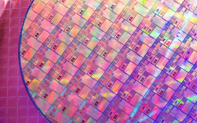
Silicon wafers are thin slices of highly pure crystalline Silicon, used in the production of integrated circuits. This article delves into the fascinating world of silicon wafers, unraveling their production process, unique properties, and the wide range of applications that make them indispensable.
Puntozero redesigned the cold plate of the power electronics of Dynamis PRC’s electric race car for additive manufacturing. The result was a 25% lighter liquid-cooled heat sink and bioinspired flow guides that increased the heat transfer surface area by 300%.

5 minutes read
The article covers the basics of TinyML, a technology that improves the privacy, energy efficiency, affordability and reliability of devices utilising artificial intelligence. Be a part of TinyML for good, an online event and showcase of ideas that aims at exploring the topic in more detail.
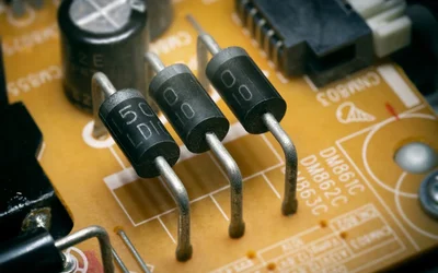
Understanding forward bias vs reverse bias configurations in diodes, exploring the theoretical aspects, implementation, applications, and considerations while noting the key differences between forward bias vs reverse bias operating modes in diodes.
A critical flaw in random number generators puts the security of billions of low-cost IoT devices at risk. This means a new approach for generating random numbers is needed, which can be found in extracting entropy from SRAM behaviour.

4 minutes read
In this episode, we talk about a blind cane from Stanford University that borrows self-driving tech to increase the mobility of visually-impaired people by 20% as well as an effort from Texas A&M to develop enhanced touchscreens which will enable users to feel textures on their smart devices.

Get to know the differences between memory options and the trade-offs you need to make when working with Bluetooth Low Energy development projects.
3 minutes read
The collaboration between Nordic Semiconductor and Edge Impulse provides resource-optimized IoT devices with more accessible machine learning at the edge.
3 minutes read
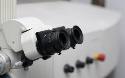
Since its debut in the 1980s, Atomic Force Microscopy (AFM) has transformed microscopic imaging and sample analysis. This article provides an essential guide to AFM, covering its core principles, functionalities, and wide-ranging applications in scientific research.
Tapis Magique is a pressure-sensitive, knitted electronic textile carpet that generates 3D sensor data based on body gestures and drives an immersive sonic environment in real time.
To address the existing barriers to IoT growth and adoption and breathe new life into the smart home market, members of the Connectivity Standards Alliance (formerly Zigbee Alliance) have launched 'Matter' (formerly Project Connected Home Over IP or Project CHIP).
4 minutes read
With the advent of powerful gateways providing both NB-IoT and LoRaWAN options, utilities need no longer exclusively select one cloud connectivity solution over another.
3 minutes read