GaN HEMT: Gallium Nitride Power Transistors
Understanding the device physics, trade-offs, and design guidance for power electronics

18 Jun, 2026. 13 minutes read

GaN HEMT: Gallium Nitride Power Transistors
Understanding the device physics, trade-offs, and design guidance for power electronics.
Key Takeaways
A GaN HEMT is a lateral wide-bandgap power transistor built around an AlGaN/GaN heterostructure and a polarization-induced 2DEG channel.
The main power electronics value proposition is low RDS(on), low charge, high switching speed, and high power density, especially from 40 V to 650 V classes.
Native GaN HEMTs are depletion mode, or normally on. Commercial power devices solve this with enhancement-mode p-GaN gates or cascode structures using a low-voltage silicon MOSFET.
GaN is not a drop-in MOSFET in every design. Gate-drive accuracy, dv/dt control, layout inductance, thermal path, and dynamic on-resistance must be deliberately designed.
GaN competes strongly against silicon MOSFETs in high-frequency AC-DC and DC-DC converters, while SiC MOSFETs and IGBTs remain dominant above the mainstream 650 V GaN range.
EPC, Infineon, Navitas, Texas Instruments, and Transphorm all offer real GaN power devices or integrated circuits, and their evaluation boards can reduce early design risk.
Introduction
A GaN HEMT, short for gallium nitride high electron mobility transistor, is one of the most important wide-bandgap semiconductor devices now used in compact power electronics. The device combines a high-critical-field semiconductor with a high-mobility electron channel, enabling power converters to switch faster and dissipate less energy than comparable silicon solutions when the surrounding circuit is properly designed. This is why GaN HEMTs appear in USB-C fast chargers, server power supplies, telecom rectifiers, solar and energy storage converters, robotics power stages, LiDAR pulsers, and selected motor drives.
The physics matters because the engineering tradeoffs follow directly from it. A GaN HEMT does not conduct through an inverted MOS channel like a silicon MOSFET. It conducts via a two-dimensional electron gas (2DEG) formed at an AlGaN/GaN heterointerface. That channel gives high electron mobility and low charge, while the approximately 3.43 eV bandgap and roughly 3.3 MV/cm critical electric field of GaN give high blocking capability for a thin lateral drift region. Public-domain bandgap property tables list GaN at a 3.43 eV bandgap, 3300 kV/cm breakdown field, 1500 cm²/V·s electron mobility, and 1.3 W/cm·K thermal conductivity, compared with silicon at 1.12 eV, 300 kV/cm, 1300 cm²/V·s, and 1.5 W/cm·K.
This article explains what GaN HEMTs are, how they work, and when engineers should use them. It also addresses the practical limitations directly: enhancement-mode gate design, cascode behavior, dynamic RDS(on), current collapse, QFN and top-side cooling, switching losses, EMI, evaluation boards, and the boundary between GaN, silicon MOSFETs, SiC MOSFETs, and IGBTs.
What Is a GaN HEMT?
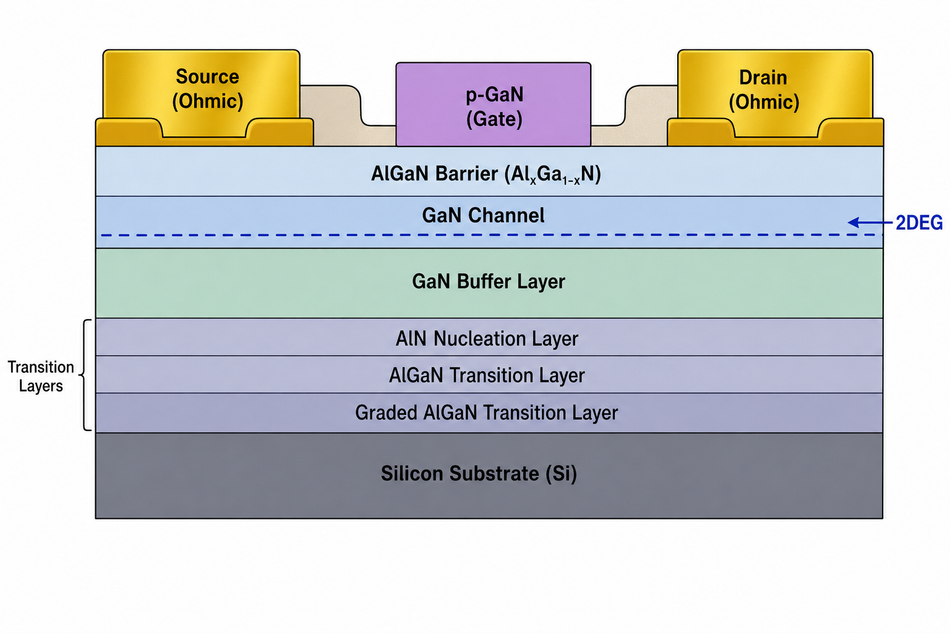
A high-electron-mobility transistor is a field-effect transistor that uses a heterostructure to form a high-mobility conduction channel. In power GaN devices, the most common structure is a lateral AlGaN/GaN HEMT. The source and drain sit on the top side of the die; the current flows laterally through the 2DEG, and the breakdown voltage is set largely by the gate-to-drain access region, field plates, passivation, and buffer design.
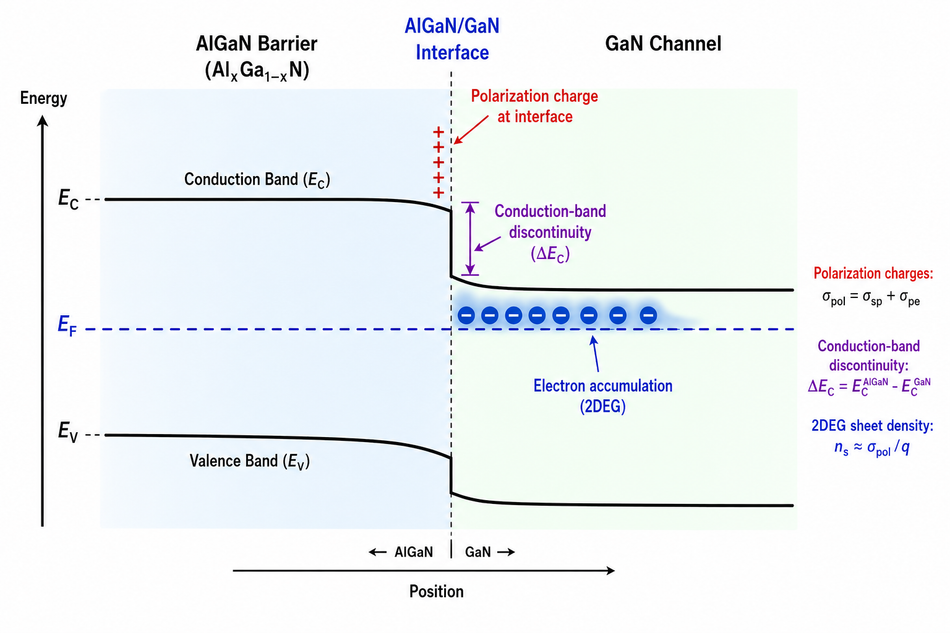
The 2DEG is the defining feature. AlGaN and GaN have different band gaps, lattice constants, and polarization fields. In Ga-face AlGaN/GaN structures, spontaneous and piezoelectric polarization create sheet charge near the interface. Electrons accumulate in a narrow quantum well on the GaN side of the interface, forming a two-dimensional electron gas without the intentional channel doping used in many silicon devices.
This channel is useful because it avoids ionized-impurity scattering in the conduction path, supports high sheet-carrier density, and can be depleted or enhanced by the gate electric field.
Suggested Reading: Where GaN can, it should, and GaN can in more and more places
Material Properties: GaN vs Si and SiC
The table below gives a device-selection view of the material physics. These values are not a replacement for a datasheet, but they explain why wide bandgap semiconductors enable smaller, faster, higher-efficiency converters.
Property | Silicon | 4H-SiC | GaN | Engineering meaning |
Bandgap energy | 1.12 eV | 3.26 eV | 3.43 eV | Wider bandgap supports high-temperature and high-field operation. |
Breakdown field | 300 kV/cm | 2200 kV/cm | 3300 kV/cm | Higher field enables thinner blocking regions and lower resistance. |
Electron mobility | 1300 cm²/V·s | 950 cm²/V·s | 1500 cm²/V·s | GaN combines wide bandgap with high electron transport. |
Saturation velocity | 1.0 x 10⁷ cm/s | 2.0 x 10⁷ cm/s | 2.2 x 10⁷ cm/s | High velocity helps high-frequency operation. |
Thermal conductivity | 1.5 W/cm·K | 3.8 W/cm·K | 1.3 W/cm·K | SiC has the stronger bulk heat-spreading advantage. |
GaN's high electrical performance does not automatically mean easier thermal design. Bulk silicon carbide has higher thermal conductivity than GaN, and many commercial power GaN HEMTs are lateral devices on silicon substrates. GaN can reduce loss and shrink passive components by increasing switching frequency, but heat still must be extracted through a small die and package.
Device Structure and 2DEG Physics
A commercial GaN HEMT power device is normally grown as an epitaxial stack. Starting from the bottom, the structure often includes a silicon substrate for power HEMTs, transition layers to manage lattice and thermal expansion mismatch, a high-resistivity buffer layer, a GaN channel, an AlGaN barrier, passivation, field plates, and metal source, gate, and drain contacts. SiC and sapphire substrates are also used in the broader GaN ecosystem, with SiC especially important in RF GaN for its thermal conductivity and lattice-matched advantages, while sapphire is common in LED manufacturing.
Epitaxial growth is usually performed by MOCVD, also called MOVPE. Precursors such as trimethylgallium, ammonia, and trimethylaluminum are used to grow GaN, AlN, and AlGaN layers. The buffer layer is more than a mechanical transition layer. It must suppress leakage, manage wafer bow and dislocations, and control trapping. Carbon or iron doping is commonly used to make GaN buffers highly resistive, but buffer traps can contribute to dynamic on-resistance and current collapse if not engineered correctly.
The AlGaN barrier is thin, often on the order of tens of nanometers. Its aluminum content and thickness affect the 2DEG sheet density, threshold voltage, access resistance, and ohmic contact behavior. A higher 2DEG density can reduce on-resistance but also make normally-off operation harder and affect electric-field management. This is why GaN device design is a coupled electrostatic, materials, and reliability problem rather than a simple scaling exercise.
Suggested Reading: Are GaN semiconductor power components ready for automotive?
Normally Off Operation: E-Mode p-GaN vs Cascode
The native GaN HEMT problem is safety. A conventional AlGaN/GaN HEMT naturally forms a conducting 2DEG at zero gate bias, so the device is depletion mode, or normally on. That is not acceptable for most power converters because loss of gate drive should turn the switch off. Commercial GaN power devices therefore use normally-off architectures.
Enhancement mode, often written as e-mode, typically refers to a p-GaN gate or a related gate structure that depletes the 2DEG beneath the gate at zero bias. Applying positive gate bias restores the channel. Infineon's CoolGaN application note states that adding a p-type gate raises the threshold voltage from negative to positive, thereby making the HEMT enhancement-mode and normally off. It also describes the conduction path as the 2DEG formed between GaN and AlGaN layers.
The alternative is a cascode configuration. In a cascode GaN FET, a low-voltage silicon MOSFET is connected with a high-voltage depletion-mode GaN HEMT so the external device behaves like a normally-off three-terminal transistor.
Architecture | How it works | Advantages | Tradeoffs |
E-mode p-GaN HEMT | p-GaN gate depletes the 2DEG at VGS = 0 V. Positive gate bias turns it on. | Native normally-off behavior, very low charge, compact packaging, strong fit for integrated GaN ICs. | Tight gate-drive window, gate stress limits are vendor-specific, layout must control ringing and false turn-on. |
Cascode GaN FET | Low-voltage Si MOSFET drives a normally-on high-voltage GaN HEMT internally. | Easier to drive with common MOSFET gate drivers, wider apparent gate margin, familiar TO-247 options. | Added silicon device affects reverse conduction, capacitance, and switching behavior. Always model the actual cascode datasheet. |
Depletion mode GaN HEMT | 2DEG conducts at zero gate bias. Negative gate voltage turns off the channel. | Useful in some RF and specialized circuits. | Not preferred as a standalone power switch for fail-safe power conversion. |
The engineering choice is not only "which is faster." It is about gate-driver availability, isolation, fault response, packaging, thermal system, source inductance, reverse-conduction interval, production qualification, and the level of application support the vendor provides.
Switching Speed, Gate Driver Design, and Layout
GaN's switching speed is both its advantage and its main integration challenge. Lower gate charge and output charge allow high-frequency operation, often hundreds of kilohertz to low megahertz in practical converters. TI's LMG3522R030-Q1 integrates a silicon driver with a 650 V, 30 mΩ GaN FET, and TI specifies adjustable slew-rate control from 20 V/ns to 150 V/ns for EMI and switching optimization.
Discrete e-mode GaN gate drive is less tolerant than classic silicon MOSFET drive. EPC's eGaN guidance provides a concrete example: EPC eGaN devices have maximum gate voltages of +6 V and -5 V, and first-generation devices were designed for 5 V drive. The same note emphasizes an accurate gate-drive supply voltage, low gate-loop impedance, low pull-down resistance, and close placement of the driver, because only about 1 V separates the 5 V recommended drive from the 6 V absolute maximum in that device family.
The practical gate driver checklist is straightforward:
Use a driver specified for GaN, not a generic MOSFET driver by default.
Keep the gate loop short, with Kelvin source return where provided.
Split turn-on and turn-off resistance if EMI and false turn-on require different impedances.
Control common-source inductance, as a few nanohenries can materially alter the effective VGS during fast current transitions.
Verify dv/dt immunity, bootstrap behavior, UVLO thresholds, Miller clamp strategy, and negative gate bias recommendations against the exact datasheet.
Confirm probe method. A long ground lead on an oscilloscope probe can create measurements that look like gate overvoltage or ringing that is partly a measurement artifact.
Reverse Conduction
Reverse conduction also differs from the behavior of silicon MOSFETs. A lateral e-mode GaN HEMT has no intrinsic body diode, so there are no minority-carrier reverse-recovery losses in the same sense as a silicon body diode.
However, reverse conduction still has voltage drop and dead-time loss, and cascode devices can have datasheet QRR values because the internal silicon MOSFET and structure influence third-quadrant behavior.
Dynamic On-resistance
Dynamic on-resistance is another GaN-specific design and qualification issue. Traps in the buffer layer, surface states, and high-field regions can temporarily increase RDS(on) after high-voltage blocking or switching stress. JEDEC JEP173 describes dynamic ON-resistance testing as a measure of charge-trapping phenomena in GaN power transistors, and JEP180.01 provides guidelines for the switching-reliability evaluation of planar e-mode, depletion-mode, integrated GaN, and cascode GaN power switches.
Suggested Reading: Gate Driver Design for Modern Power Electronics
Thermal Design, QFN Packaging, and Power Density
Power density is usually the system-level reason to choose GaN. Faster switching can reduce magnetics, capacitors, heat sinks, and enclosure size, but the transistor package must remove heat effectively.
Many GaN devices are packaged in QFN, DFN, TOLL, TOLT, LGA, BGA, embedded, or chip-scale formats rather than large leaded packages. Small packages reduce inductance, which helps switching speed, but they require more intentional thermal design.
QFN is common because it is compact, low-inductance, surface-mount-compatible, and suitable for integrated circuits. TI's 650 V LMG352x family uses a 12 mm x 12 mm x 0.9 mm top-side cooled QFN power-stage package with an exposed copper thermal pad on the side opposite the mounting pins, so a heatsink or cold plate can be attached directly to the package top. TI states that this avoids the printed-circuit-board thermal impediment associated with purely bottom-side cooling.
Bottom-cooled QFN devices still work well when the PCB is treated as part of the thermal stack. TI's LMG341x thermal note states that its GaN power stages use low-inductance QFN packages to avoid long-lead and bond-wire inductance and gives a typical junction-to-case thermal resistance of 0.5 °C/W, with heat transferred through the thermal pad into PCB copper, vias, TIM, and heatsink.
GaN vs Silicon MOSFETs vs SiC MOSFETs
GaN should be selected by topology and voltage class, not by material enthusiasm. Silicon MOSFETs still dominate cost-sensitive low-frequency designs and very low voltage rails. SiC MOSFETs dominate many 800 V bus, 1200 V, traction, solar, and high-power industrial applications. IGBTs remain relevant where cost, ruggedness, and high current at lower switching frequency matter.
TI's GaN versus SiC comparison places SiC devices at voltage levels as high as 1200 V with high current capability for traction inverters, high-power solar farms, and large three-phase grid converters. It describes GaN FETs as typically 600 V devices suited to high-density converters around 10 kW and higher, including consumer, server, telecom, industrial power supplies, servo drives, grid converters, EV onboard chargers, and DC/DC converters.
Selection factor | Silicon MOSFETs and Si MOSFETs | GaN HEMTs | SiC MOSFETs |
Common voltage fit | Very strong below 200 V, available into superjunction 600 V and 650 V classes. | Strong at 40 V, 80 V, 100 V, 200 V, and 650 V classes. | Strong at 650 V, 750 V, 900 V, 1200 V, 1700 V and above. |
Switching frequency | Good at low and moderate frequencies, limited by Qg, Qoss, and reverse recovery in many high-voltage hard-switching stages. | Excellent at high frequency because of low charge and no body-diode reverse recovery in e-mode lateral devices. | Faster than IGBT and many silicon MOSFETs, but usually not as fast as GaN at comparable power. |
Switching losses | Can be high in hard-switched high-voltage bridges. | Often lowest in 650 V totem-pole PFC, LLC, active clamp flyback, and high-frequency DC-DC converters. | Excellent in high-voltage, high-power converters, especially where voltage and temperature are high. |
Gate drive | Mature, broad driver ecosystem, often 10 V or 12 V for MOSFETs. | Tight, vendor-specific gate voltage window or integrated driver. Layout is critical. | Typically 15 V to 20 V on and negative off bias may be used in demanding designs. |
Thermal behavior | Mature packages, broad SOA, avalanche often rated. | Low loss but compact thermal path. Dynamic RDS(on) and package heat spreading matter. | Strong bulk thermal conductivity and rugged high-voltage packages. |
Cost and maturity | Lowest cost and broadest supply. | Maturing fast, often lower system cost when passive components and cooling shrink. | Mature in EV traction and solar, but substrate and device cost are higher. |
Best application fit | Low-cost supplies, low-voltage DC rails, low-frequency designs. | Fast chargers, adapters, telecom, server power, high-frequency PFC, DC-DC converters, LiDAR, compact motor drives. | EV traction, high-power solar, grid converters, industrial drives, high-voltage battery systems. |
Recommended Reading: SiC MOSFET: Wide-bandgap Power Devices for High-Efficiency Converters.
Real Devices, Vendors, and Platforms
The commercial GaN ecosystem is now broad enough that engineers should compare platforms, not only transistor ratings.
EPC focuses strongly on low-voltage and mid-voltage eGaN FETs and ICs. EPC states that its off-the-shelf product portfolio spans 15 V to 350 V, and the EPC2304 is a 200 V, 5 mΩ enhancement-mode GaN power transistor in a 3 mm x 5 mm package for synchronous rectification, AC/DC chargers, high-frequency DC-DC conversion, motor drives, class-D audio, wireless power, LiDAR, and multilevel PFC. EPC lists evaluation boards such as EPC90140, EPC9196, and EPC91107 for the EPC2304 platform.
Infineon, including the acquired GaN Systems business, offers CoolGaN devices and a broader power portfolio. Infineon's IGT65R035D2 page describes a 650 V e-mode CoolGaN G5 transistor in a bottom-side-cooled TOLL package, with ultrafast switching, no reverse-recovery charge, low dynamic RDS(on), reverse-conduction capability, and JEDEC qualification to JESD47 and JESD22.
Texas Instruments emphasizes integrated GaN power stages. The automotive LMG3522R030-Q1 integrates a 650 V, 30 mω GaN FET with driver, protection, and temperature-reporting capabilities. TI lists cycle-by-cycle overcurrent protection, latched short-circuit protection support on its EVM, and adjustable slew rate from 20 V/ns to 150 V/ns.
Transphorm's cascode platform remains important for engineers who prefer more MOSFET-like gate drive. The TP65H035WS is a 650 V normally-off cascode GaN FET in TO-247, with a datasheet topology recommendation of up to 3770 W in CCM bridgeless totem-pole PFC and up to 4600 W in a hard-switched inverter under stated conditions. These are not universal power limits, but they are useful examples of the class of applications targeted by 650 V cascode GaN.
Applications and Engineering Fit
Fast chargers and adapters are the most visible applications of GaN. Active clamp flyback, quasi-resonant flyback, LLC, and totem-pole PFC stages benefit from lower switching losses and smaller magnetics. The higher switching frequency allows for smaller transformers, inductors, and capacitors, which is why compact 65 W to 300 W USB-C supplies became a high-volume segment in the GaN market.
Data Centers and Telecom Sector
Data center and telecom power are strong fits because efficiency and power density both monetize directly. Common examples include 48 V bus conversion, 400 V to 48 V intermediate bus converters, CRPS power supplies, PFC stages, and high-frequency isolated DC-DC converters. Navitas and TI both explicitly target data center, telecom, and high-density power conversion with integrated GaN platforms.
Drives and Actuators
Motor drives are more mixed. Low-voltage BLDC stages, robotics actuators, drones, e-bikes, servo drives, and compact integrated motor controllers can benefit from high switching speed and small filters. For long-cable industrial drives, traction inverters, or high-current 800 V systems, dv/dt, insulation stress, EMI, short-circuit ruggedness, and voltage class often push the design toward SiC MOSFETs or IGBTs. EPC's 200 V devices target BLDC motor drives and robotics, while TI and Navitas position 650 V GaN for onboard chargers, DC-DC converters, and selected motor-drive use cases.
LiDAR and High Frequency Circuits
LiDAR and RF use the same material family but different design priorities. LiDAR pulsers want nanosecond-scale current pulses with low inductance and high peak current. RF GaN HEMTs, often GaN-on-SiC, are optimized for gain, power-added efficiency, linearity, and thermal behavior at microwave frequencies.

Power GaN HEMTs are optimized for blocking voltage, RDS(on), switching charge, ruggedness, and package integration. The device physics overlaps, but the datasheets and qualification methods are not interchangeable.
Suggested Reading: LiDAR: making significant inroads into our factories and warehouses
Conclusion: Where GaN HEMTs Are Headed
GaN HEMTs are no longer exotic, but they are still engineering devices rather than commodity MOSFET replacements. Their strength comes from a lateral AlGaN/GaN heterostructure, a polarization-induced 2DEG, high electron mobility, low charge, and the wide bandgap of gallium nitride. In the right voltage and topology, these properties translate into very low switching losses, smaller passive components, and high power density.
The realistic market boundary is important. Mainstream power GaN HEMTs are concentrated in low-voltage classes such as 40 V to 200 V and high-voltage classes around 600 V to 650 V. SiC MOSFETs and IGBTs remain the default technologies for many higher-voltage, high-current, and harsh industrial systems. Future trends include more integrated circuits with drivers and protection, better top-side cooled QFN and TOLL packages, more robust short-circuit behavior, improved dynamic RDS(on), bidirectional GaN switches, 200 mm and potentially 300 mm GaN-on-silicon manufacturing, and early vertical GaN research for voltage classes beyond the lateral device mainstream.
FAQ
1. What is a GaN HEMT?
A GaN HEMT is a gallium nitride high electron mobility transistor that conducts through a 2DEG formed at an AlGaN/GaN heterointerface. Unlike a silicon MOSFET, which uses a MOS inversion channel, a GaN HEMT uses polarization-induced charge and a lateral channel. In power electronics, the result is a fast switch with low charge, low RDS(on), and strong performance in compact high-frequency converters.
2. Why do GaN HEMTs switch faster than silicon MOSFETs?
GaN HEMTs switch faster because their lateral 2DEG channel and device geometry produce low gate charge, low output charge, and no intrinsic silicon-style body diode reverse recovery in e-mode devices. Lower charge means the gate driver and resonant or hard-switching node need less energy per transition. The result can be higher switching frequency, smaller passive components, and lower switching losses when layout and EMI are controlled.
3. Are GaN HEMTs normally on or normally off?
The native AlGaN/GaN HEMT is normally on because the 2DEG exists at zero gate bias. Commercial power devices are normally off through enhancement mode gate structures, usually p-GaN, or through a cascode arrangement that pairs a depletion-mode GaN HEMT with a low-voltage silicon MOSFET. Engineers should verify the exact threshold, gate limits, and failure behavior, as e-mode and cascode devices behave differently.
4. What voltage range is practical for power GaN?
Commercial power GaN is strongest in low-voltage and mid-voltage classes such as 40 V, 80 V, 100 V, 200 V, and in high-voltage offline classes around 600 V to 650 V. Some devices list transient ratings above their continuous VDS rating, but that should not be treated as a higher steady-state design class. For 1200 V traction, grid, and heavy industrial systems, SiC MOSFETs and IGBTs are usually more mature choices.
5. What is dynamic RDS(on) in GaN HEMTs?
Dynamic RDS(on) is the temporary increase in on-resistance after the device has experienced high voltage, high field, or switching stress. It is related to charge trapping in buffer layers, surface states, and field-plate regions. This effect is also called current collapse in some contexts. Designers should review vendor dynamic RDS(on) data, JEDEC JEP173 test methods, double-pulse results, and application-specific switching stress.
6. What are the biggest layout risks with GaN HEMTs?
The biggest layout risks are excessive gate-loop inductance, common-source inductance, poor power-loop minimization, inadequate Kelvin source routing, noisy bootstrap or bias supply design, and probing artifacts. Fast dv/dt can create false turn-on, ringing, EMI, and device overstress. A proven evaluation board is often the fastest way to learn the vendor's preferred layout before designing a production half bridge or converter.
References
PowerAmerica, How Wide Bandgap (WBG) Works
Texas Instruments, LMG3522R030-Q1 Automotive 650-V 30-mΩ GaN FET with integrated driver, protection and temperature reporting
Texas Instruments, Wide-bandgap semiconductors: Performance and benefits of GaN versus SiC, Analog Design Journal
JEDEC JEP180.01, Guideline for Switching Reliability Evaluation Procedures for Gallium Nitride Power Conversion Devices
EPC, Gallium Nitride (GaN) FETs and ICs Product Selector Guide
in this article
1. Key Takeaways2. Introduction3. What Is a GaN HEMT?4. Material Properties: GaN vs Si and SiC5. Device Structure and 2DEG Physics6. Normally Off Operation: E-Mode p-GaN vs Cascode7. Switching Speed, Gate Driver Design, and Layout8. Thermal Design, QFN Packaging, and Power Density9. GaN vs Silicon MOSFETs vs SiC MOSFETs10. Real Devices, Vendors, and Platforms11. Applications and Engineering Fit12. Conclusion: Where GaN HEMTs Are Headed13. FAQ14. References