Featured
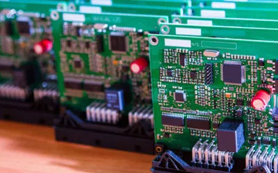
With today’s most advanced cloud manufacturing platforms, users can access the full capabilities needed to move seamlessly between prototyping, testing, and full-scale production

With today’s most advanced cloud manufacturing platforms, users can access the full capabilities needed to move seamlessly between prototyping, testing, and full-scale production
PCB Trace Width Calculator
Glossary of Semiconductors Terms
With today’s most advanced cloud manufacturing platforms, users can access the full capabilities needed to move seamlessly between prototyping, testing, and full-scale production
Rapid PCBA prototyping using electronics cloud manufacturing offers many advantages including problem identification, reduced error rate, lower costs, and shortened manufacturing timelines.
A team of researchers in Korea has been working on functional acoustic energy transmission (AET) systems, and their latest paper details a major breakthrough: Prototypes capable of powering LEDs, sensors, and Bluetooth transmitters at range and through materials include metal, tissue, and water.
Semiconductors are the building blocks of modern electronics, powering everything from smartphones to satellites. This in-depth guide provides a comprehensive understanding of semiconductors' engineering principles and applications, delving into their fundamental concepts, materials, devices, manufacturing processes, and their impact on today's technology landscape.
18 minutes read.
20 minutes read.
26 minutes read.
17 minutes read.
21 minutes read.
29 minutes read.

Semiconductors
Nordic Semiconductor is a fabless semiconductor company specializing in wireless technology that powers the IoT.
181 Posts
Exploring the shift to additive digital printing in modern electronics fabrication.
This article explains the ESP8266 pinout, covering GPIO mapping, boot-strapping pins, safe-to-use pins, flash connections, ADC limits, deep-sleep functions, and NodeMCU and D1 mini pin labels.
Learn how a Hall Effect Current Sensor works, including principles, topologies, specifications, comparisons and engineering applications.
A guide covering the full radio-frequency design workflow, starting from setting specifications and choosing topologies to matching, simulation, layout, and verification, to help antenna engineers.
Controlled impedance is the control of PCB trace impedance within specified tolerances. This article covers microstrip and stripline designs, IPC-2141A formulas, stackup selection, impedance tolerances, routing practices, and TDR testing for signal integrity.
Exploring the shift to additive digital printing in modern electronics fabrication.
A PCB design can be electrically correct, pass every design rule check and perform exactly as expected on an engineer's screen - and still cause significant problems when it reaches manufacturing.
A semiconductor is a material whose electrical conductivity falls between that of a conductor and an insulator and can be controlled by temperature, light, and impurities. This article covers semiconductor materials, doping, diodes, transistors, and integrated circuits.
With today’s most advanced cloud manufacturing platforms, users can access the full capabilities needed to move seamlessly between prototyping, testing, and full-scale production

4 minutes read
Rapid PCBA prototyping using electronics cloud manufacturing offers many advantages including problem identification, reduced error rate, lower costs, and shortened manufacturing timelines.
4 minutes read
A team of researchers in Korea has been working on functional acoustic energy transmission (AET) systems, and their latest paper details a major breakthrough: Prototypes capable of powering LEDs, sensors, and Bluetooth transmitters at range and through materials include metal, tissue, and water.
In this tutorial series it is all about the procedure of creating realistic renders from 3D models of PCBs in Blender. In the third (and last) part of this tutorial series, we will take a look at different steps that will lead to a better render result.

4 minutes read
The IC manufacturing lifecycle is the foundation of IoT security.
Engineers have developed a glucose power source that could fuel miniature implants and sensors.
Beyond leisure, drones offer enormous potential for developing a wide array of innovative applications that benefit society.

3 minutes read
Understanding the basics of functional safety.
As an electronics engineer, you need to ensure PCBA documentation is clean, complete, and up to date. Here are MacroFab's tips to help you overcome common documentation challenges that can keep your designs from reaching their maximum production potential
4 minutes read
Cellular IoT in both its LTE-M and NB-IoT flavors took longer than competing proprietary Local Wide Area (LWA) network technologies to come to market. As a direct result of this, they lost a lot of early market share.
4 minutes read
Relying on single-sourced components is a risky move that constricts your supply chain options and pins your product's future to one option. What happens if that option disappears? We have tips that can protect you from single-sourcing uncertainty.
4 minutes read
In this tutorial series it is all about the procedure of creating realistic renders from 3D models of PCBs in Blender. The first part covers the preparation of the 3D objects, the required textures and UV unwrapping.
5 minutes read
MIT engineers have developed a paper-thin loudspeaker that can turn any surface into an active audio source.
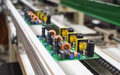
Electronic product development is a highly iterative process that involves going back and forth between the design and manufacturing stages. Cloud Manufacturing Services make it possible for engineers to focus on innovation.
IoT infrastructure has many weak spots which demand robust security assurance methods.