Forward Bias, Reverse Bias and their effects on Diodes
Understanding forward bias vs reverse bias configurations in diodes, exploring the theoretical aspects, implementation, applications, and considerations while noting the key differences between forward bias vs reverse bias operating modes in diodes.

Last updated on 25 Mar, 2024. 17 minutes read
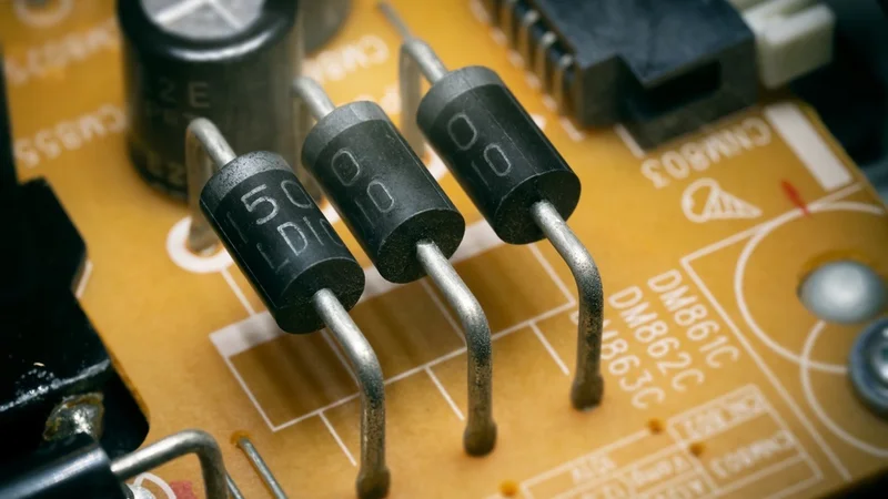
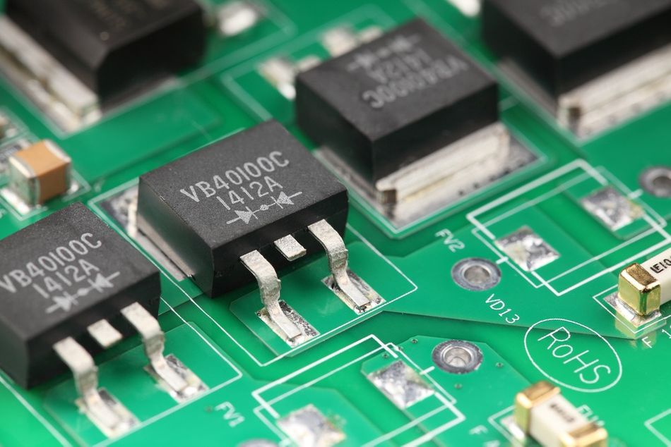
Three Diodes placed on a PCB
Introduction
Diodes are essential components in electronic circuits, playing a crucial role in controlling the flow of electrical current. These semiconductor devices are designed to allow current to flow easily in one direction while restricting it in the opposite direction. This unique property makes diodes indispensable in a wide range of applications, from power supply rectification to signal conditioning and protection circuits.
This article will focus on the two primary operating modes of diodes - Forward bias vs Reverse bias.
What is a Diode?
A Diode is a fundamental semiconductor device that not only serves as a basic circuit element but also provides the template for the development of many critical electronic devices like transistors, power diodes, LEDs, etc.
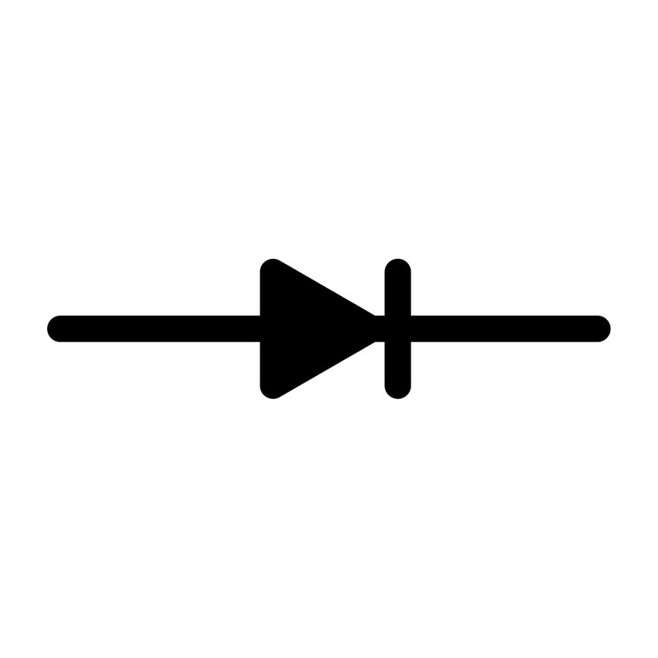
It is a two-terminal electronic component that consists of a P-N junction, formed by joining a p-type semiconductor and an n-type semiconductor. This junction allows current to flow easily in one direction, known as the forward direction, while restricting current flow in the opposite direction, called the reverse direction. In circuit diagrams, a diode is represented by a triangle pointing towards a straight line, with the triangle indicating the direction of easy current flow (forward direction).
Essentially, the function of a diode in electronic circuits is to control the direction of current flow. When a diode is forward-biased, meaning that the positive terminal (anode) is connected to a higher potential than the negative terminal (cathode), it allows current to flow through it with minimal resistance. In a reversed polarity, the diode is said to be reverse-biased, where it blocks the current flow, acting as an open switch.
This unidirectional current flow property makes diodes essential for various applications, such as rectification, where they convert alternating current (AC) to direct current (DC), and in protection circuits, where they prevent reverse currents from damaging sensitive components.
P-N Junction and Doping
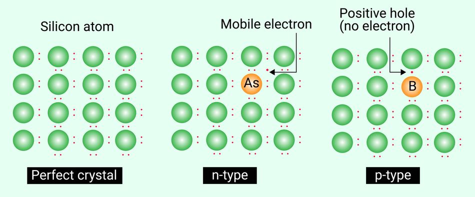
A P-N junction is formed when a p-type semiconductor, which has an excess of holes (positive charge carriers), is joined with an n-type semiconductor, which has an excess of electrons (negative charge carriers).
- Mixing Silicon (Si) or Germanium (Ge) with trivalent impurities such as Boron (B), Aluminum (Al), Galium (Ga), or Indium (In) produces a p-type semiconductor.
- Mixing Silicon (Si) or Germanium (Ge) with pentavalent impurities like Phosphorus (P), Arsenic (As), or Stibium (Si) produces an n-type semiconductor.
The process of mixing impurities is called Doping.
Recommended Reading: Understanding N-Type vs P-Type Semiconductors
When these two types of semiconductors are brought together, the excess electrons from the n-type material diffuse into the p-type material, while the excess holes from the p-type material diffuse into the n-type material. This diffusion process creates a region near the junction called the depletion region, also known as the potential barrier.
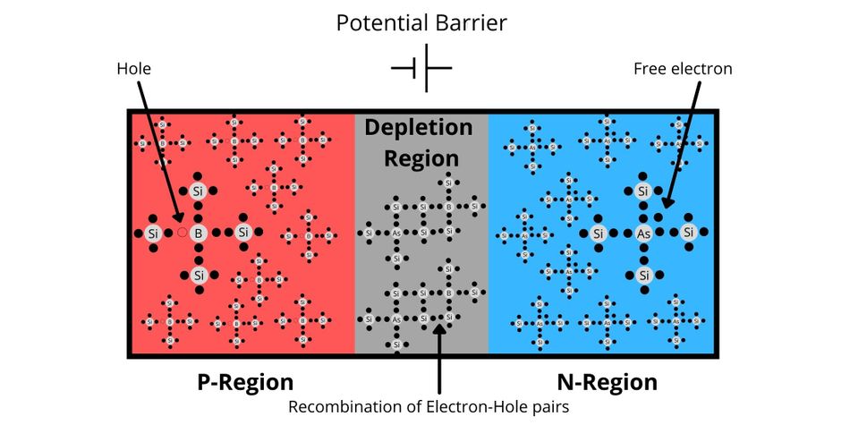
This potential barrier prevents the majority of carriers from crossing the junction under equilibrium conditions. Hence, the charged particles would require an additional force (voltage) to cross this barrier from now on due to a newly created obstruction. For a Silicon (Si) p-n junction, the typical value of this barrier is 0.7 V, and for p-n junctions developed with Germanium (Ge), it's 0.3 V.
The potential barrier is essential for the operation of a diode, as it determines the voltage required to forward-bias the diode and allow current to flow through it. When the applied forward voltage exceeds the potential barrier, the depletion region narrows, and the diode conducts current. Conversely, when the diode is reverse-biased, the potential barrier increases and the depletion region widens, preventing current flow.
Diode Characteristics
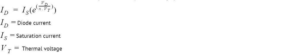
The current-voltage (I-V) characteristics of a diode describe the relationship between the current flowing through the diode and the voltage applied across it. In the forward bias region, this relationship is non-linear and closely follows the following equation, also known as the Shockley diode equation.
The Practical Diode
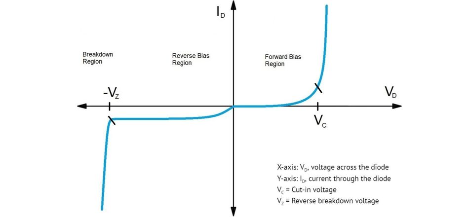
Fig 4 shows a typical IV characteristic of a practical diode. We can break down the figure as follows:
In the forward-biased region, the current increases exponentially with the applied voltage due to a small forward resistance.
In the reverse-biased region, the current remains close to zero until the reverse breakdown voltage is reached
The threshold voltage, also known as the cut-in voltage ‘Vc ‘ or forward voltage drop, is the minimum voltage required to forward-bias a diode and allow significant current to flow through it. The threshold voltage varies depending on the type of diode and the semiconductor material used. Light-emitting diodes (LEDs) have higher threshold voltages, ranging from 1.7 V to 3.3 V, depending on the colour of the emitted light.
The Ideal Diode
The ideal diode model is a simplified representation of a diode's behavior, which assumes that the diode has zero resistance in the forward-biased region and infinite resistance in the reverse-biased region. In this model, the diode acts as a perfect conductor when forward-biased and a perfect insulator when reverse-biased.
However, real diodes deviate from this ideal behavior. In the forward-biased region, diodes have a small forward resistance, leading to a voltage drop across the diode. In the reverse-biased region, diodes have a small leakage current, which is usually negligible but can become significant at high temperatures or near the reverse breakdown voltage.
Additionally, the ideal diode model does not account for the reverse recovery time, which is the time required for a diode to switch from the conducting state to the non-conducting state when the bias changes from forward to reverse.
Forward Bias
What is Forward Bias?
When the positive terminal of a diode is connected to a higher potential and the negative terminal is connected to a lower potential, the diode is said to be forward-biased. Hence, the applied voltage is in the same direction as the diode's forward voltage drop, allowing current to flow through the diode with minimal resistance.
Forward Bias and Depletion Region
As the applied voltage increases, the depletion region becomes narrower, as the electric field created by the applied voltage begins to neutralize the electric field created by the immobile ions. This reduction in the depletion region width allows more majority carriers to cross the junction, resulting in an exponential increase in current flow through the diode.
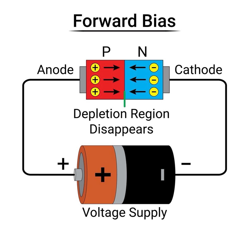
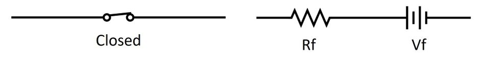
At this point, a practical diode can be modelled as a series combination of a voltage source in series with a resistor. The value of the voltage is extremely small and is equal to the cut-in voltage. Likewise, the resistance has a small magnitude.
In case of an ideal diode which has no resistance, forward bias can be modeled as a closed switch.
Current Flow in Forward Bias
When a diode is forward-biased, current flows through the device from the anode to the cathode. Due to this flow of current, the voltage developed across the diode is given as:

Since the value of resistance is low, the IdRf term doesn’t change significantly. Coming to the forward voltage drop Vf, let I1 and I2 be the diode currents corresponding to the applied diode voltages V1 and V2 across two diodes.
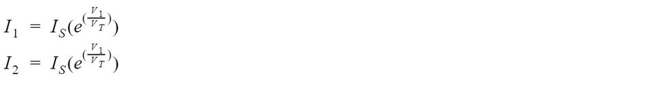
The ratio of the equations give,

Which can be rewritten as:

The voltage/current difference equation suggests that even for a drastic change in the value of current, the voltage drop across the diode will be minimal, a simple consequence of a logarithmic relationship.
Hence, during the forward-bias analysis of a diode, the following information can be inferred:
- The on-state voltage drop can be considered constant for a reasonably significant change in diode current.
- The relationship between the applied voltage and the current flow in a forward-biased diode is exponential and can be described by the Shockley diode equation. which states that the current is proportional to the exponential of the applied voltage divided by a constant (the thermal voltage).
- The exponential relationship results in a rapid increase in current once the applied voltage exceeds the threshold voltage.
Applications of Forward Bias
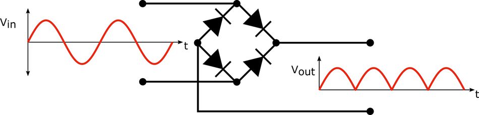
Forward bias configurations are widely used in electronic circuits. They are used when there is a need to flow signals within the circuits. Rectifier circuits are the most common examples of forward bias applications.
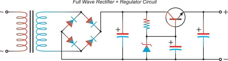
Rectifier Circuits
Rectifier circuits convert AC (alternating current) to DC (direct current). The forward-biased diodes in rectifiers act like one-way streets for the current.. This configuration allows current to flow easily through the diode, enabling rectification of the AC signal. During the AC cycle when the voltage reverses, the diode becomes reverse-biased, blocking current flow and effectively removing the negative portion of the waveform, resulting in a pulsating DC output.
.
Reverse Bias
What is Reverse Bias?
When the positive terminal of a diode is connected to a lower potential and the negative terminal is connected to a higher potential, the diode is said to be reverse-biased.
In this configuration, the applied voltage is in the opposite direction of the diode's forward voltage drop, preventing current from flowing through the diode.
Under reverse bias, the polarity of the applied voltage reinforces the built-in potential barrier of the diode.
A reverse-biased diode can be modeled as a high resistance for a practical diode, or an open-circuit ideal diode.
Effect of Reverse Bias on Depletion Region
As the applied voltage increases, the depletion region becomes wider, as the electric field created by the applied voltage attracts more majority carriers away from the junction. This widening of the depletion region increases the resistance of the diode, effectively making it an insulator.
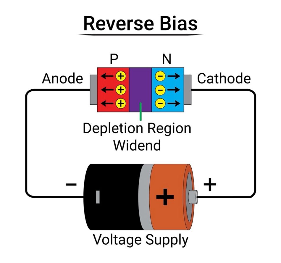
Likewise, the potential barrier also increases under reverse bias, preventing the majority carriers from crossing the junction and participating in the conduction of current. This results in a very small leakage current, typically in the range of nanoamperes (nA) or microamperes (μA), flowing through the diode under reverse bias conditions.
Leakage Current Flow in Reverse Bias
In a reverse-biased diode, the current flow is extremely small and is referred to as the leakage current or reverse saturation current. This leakage current is caused by the minority carriers (electrons in the p-type region and holes in the n-type region) that are generated thermally and can diffuse across the depletion region.
The magnitude of the leakage current is typically in the range of nanoamperes (nA) or microamperes (μA), which is much smaller than the current flowing through a forward-biased diode. A couple of factors contribute to leakage currents:
- Temperature - At higher temperatures, more minority carriers are generated thermally, increasing the leakage current. The leakage current approximately doubles for every 10°C rise in temperature.
- Junction Area - Larger junction areas result in higher leakage currents, as there are more minority carriers available to diffuse across the depletion region.
- Semiconductor Type - Germanium diodes have higher leakage currents than silicon diodes due to germanium's smaller bandgap energy.
Reverse Breakdown Region
When the reverse voltage applied to a diode increases, the leakage current remains relatively constant until a certain voltage is reached. This point is called the reverse breakdown voltage, where the leakage current suddenly increases dramatically. The sudden increase in current is due to the avalanche multiplication of minority carriers in the depletion region, leading to a large current flow through the diode.
Operating a diode beyond its reverse breakdown voltage can cause permanent damage to the device, as the high current and associated heat dissipation can degrade or destroy the diode's junction.
However, some specialized diodes, such as Zener diodes and avalanche diodes, are designed to operate in the reverse breakdown region for voltage regulation and protection applications. These diodes have well-defined and controlled reverse breakdown voltages, allowing them to be used in circuits that require stable voltage references or protection against voltage spikes.
Applications of Reverse Biased Diodes
Reverse-biased diodes find applications in various electronic circuits, leveraging their unique properties in the reverse bias condition.
Voltage Multiplier Circuits
One common application is in voltage multiplier circuits, where reverse-biased diodes are used in conjunction with capacitors to increase the input voltage to a higher level. In these circuits, the diodes act as switches, allowing current to flow in one direction during the charging phase and preventing current flow in the opposite direction during the discharging phase.
By cascading multiple stages of diodes and capacitors, voltage multiplier circuits can generate high voltages from a lower input voltage, making them useful in applications such as high-voltage power supplies, X-ray machines, and particle accelerators.
Protection Circuits
Reverse-biased diodes are used in protection circuits to prevent damage to sensitive components from voltage spikes or reverse polarity connections. For example, in a circuit with a polarized component such as an electrolytic capacitor, a reverse biased diode can be placed in parallel with the component to provide a safe discharge path in case the polarity of the applied voltage is accidentally reversed.
Similarly, in circuits exposed to voltage spikes or transients, such as in automotive systems or industrial equipment, reverse biased diodes can be used to clamp the voltage to a safe level, protecting the downstream components from damage.
Some more applications of reverse biased diodes include their use in
Peak detectors, where they help to hold the peak value of a signal
RF (radio frequency) mixers and detectors, where their non-linear characteristics are exploited for frequency mixing and demodulation.
Comparing Forward and Reverse Bias
Forward and reverse bias are two distinct operating conditions for diodes, each with its own characteristics and effects on the device's behavior. The main differences between forward and reverse bias can be summarized in the following table.
| Characteristic | Forward Bias | Reverse Bias |
| Voltage Polarity | Anode (+) higher than Cathode (-) | Cathode (-) higher than Anode (+) |
| Current Flow | Exponential increase with voltage | Extremely small leakage current |
| Depletion Region | Becomes narrower with increase in voltage | Becomes wider with increasing voltage |
| Potential Barrier | Reduced, allowing current to flow | Reinforced, preventing current flow |
| Applications | Rectifiers, voltage clamping, LED drivers | Voltage multipliers, voltage regulators, protection circuits |
Diode Behavior in Different Bias Conditions
A diode's behavior changes drastically depending on the bias condition it is subjected to.
The ability of a diode to switch between conducting and insulating states based on the applied voltage polarity is the foundation of its use in digital circuits. Diode switching is crucial in applications such as logic gates, where diodes are used to implement Boolean functions. In these circuits, the diode's state (conducting or insulating) represents a binary value (1 or 0), allowing the creation of complex digital systems. The fast switching speed of diodes, typically in the range of nanoseconds (ns), makes them suitable for high-speed digital applications.
Examples of circuits that exploit the different bias conditions of diodes include:
Rectifier Circuits - Half wave rectifiers use a single diode, while full wave rectifiers use two diodes to convert AC to DC.
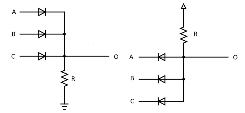
Logic Gates - Implementing AND, OR, and NOT gates by carefully selecting the resistor-diode arrangement for voltage-based logical operations.
Fig 14: Logic Gate formation with Diodes
Types of Diodes
Apart from the prominent properties that diodes exhibit under forward bias/reverse bias, they can also be designed to fulfil some other special purposes. These diodes are still made by a combination of p-type material and n-type material but can behave very differently.
Zener Diodes
Zener diodes are designed to operate in the reverse breakdown region. They are widely used for voltage regulation. When a Zener diode is reverse-biased beyond its breakdown voltage, also known as Zener Voltage, it maintains a nearly constant voltage across its terminals, even with variations in the current flowing through it. This property makes Zener diodes ideal for creating stable voltage references in power supply circuits.
By placing a Zener diode in parallel with a load, the voltage across the load can be regulated to the Zener diode's breakdown voltage, providing a stable and precise output voltage.
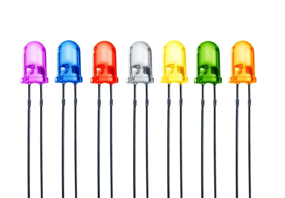
Light Emitting Diode (LED)
LEDs take the concept of current flow a step further. Just like the regular diode, when LEDs are forward-biased, both majority carriers and minority carriers participate in current conduction. In regular diodes, this process is accompanied by heat generation, but in LEDs, light is also produced.
Photodiodes
Photodiodes convert light into electricity. Their working principle is exactly the opposite to that of LEDs. When photons are incident on the junction, the electrons present in the valence band of the crystalline lattice are excited and jump to the conduction band and participate in the flow of electric current. Only if we use the photodiode in the reverse bias condition, the depletion layer will be large and allow more recombination to occur.
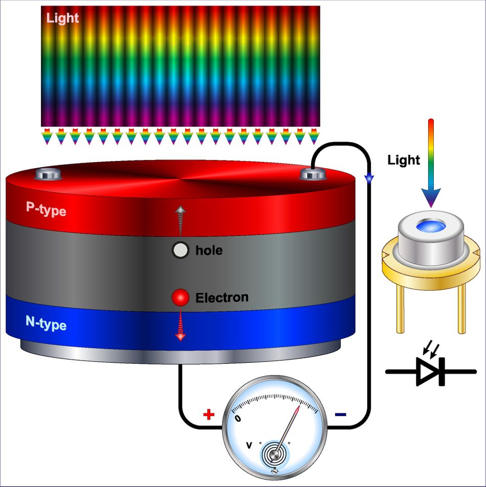
These devices can be used in automatic street lights to sense ambient light levels. Specially designed photodiodes for converting sunlight into electricity are known as solar cells and are leading the green energy revolution.
Schottky Diodes
A Schottky Diode or Schottky Barrier Diode is a special diode that can rapidly switch between conduction and blocking state depending on the forward bias voltage or reverse bias voltage applied. These diodes also have a relatively lower on-state voltage drop.
Further Reading: What is a Semiconductor? A Comprehensive Guide to Engineering Principles and Applications
Practical Considerations While Working With Diodes
While diodes are seemingly simplistic electronic components, there are a few critical aspects related to their selection, implementation, and troubleshooting. Here are a few things to consider:
Diode Selection
When selecting a diode for a specific application, several factors must be considered to ensure optimal performance and reliability.
- Forward Voltage Drop - Diodes with lower forward voltage drops are preferred in applications where power efficiency is critical, such as in battery-powered devices or low-voltage systems.
- Reverse Breakdown Voltage - The reverse breakdown voltage must be higher than the maximum expected reverse voltage in the circuit to prevent damage to the diode and ensure reliable operation.
- Max Current Rating - This parameter specifies the maximum continuous current that the diode can safely conduct without overheating or suffering damage. The maximum current rating must be higher than the expected peak current in the circuit, taking into account any transient or surge currents that may occur. Generally, most of the power rectifying diodes can work up to 1000 A.
- Safety Regulations - The safety regulation check is critical for power applications. It is important to pick diodes that have passed safety certifications such as CSA (Canada), TUV (Germany), UL (North America, and VDE, etc.
Once designers have considered these basic parameters, the following guidelines can help them safely implement diodes in their PCB designs or other circuits.
- Determine the maximum reverse voltage the diode will be subjected to and select a diode with a reverse breakdown voltage at least 20% higher than this value.
- Calculate the expected forward current in the circuit and choose a diode with a maximum current rating at least 50% higher than this value to provide a safety margin.
- Consider the forward voltage drop of the diode and select one with a lower voltage drop if power efficiency is a concern. Schottky diodes, for example, have lower forward voltage drops compared to standard silicon diodes.
- Evaluate the switching speed requirements of the application and choose a diode with an appropriate recovery time. Fast-switching diodes, such as fast recovery or ultrafast recovery diodes, are suitable for high-frequency applications.
- Take into account the operating temperature range of the circuit and select a diode with a suitable temperature rating. Some diodes, such as high-temperature or wide-bandgap diodes, are designed to operate in extreme temperature environments.
Recommended Reading: Optimizing Diode Functionality: Forward and Reverse Bias
Diode Testing and Troubleshooting
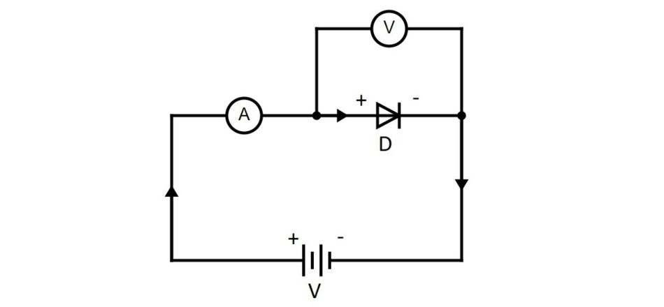
A multimeter is a valuable tool for testing diodes and can be used to determine their functionality and pinout.
To test a diode using a multimeter, set the meter to the diode test mode, which is usually represented by a diode symbol.
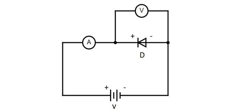
- Connect the red probe to the anode (positive terminal) and the black probe to the cathode (negative terminal) of the diode. A functional diode should display a low voltage drop, typically around 0.7 Volts for silicon diodes and 0.3 Volts for germanium diodes, in the forward bias direction.
- When the probes are reversed, the multimeter should display an open circuit or a very high resistance, indicating that the diode is not conducting in the reverse direction.
How to Determine Failed or Broken Semiconductor Diodes?
Diodes can fail in several ways, each with its own characteristic symptoms such as:
- Open Circuit - A common failure mode, where the diode does not conduct current in either direction. This can be caused by a damaged or broken junction, often due to excessive current or voltage stress.
- Short Circuit - A mode where the diode conducts current in both directions with little or no resistance. This can be caused by a manufacturing defect or by excessive reverse voltage, leading to the breakdown of the diode's junction.
- Increased Leakage Current - A condition where the diode conducts more current than expected in the reverse bias condition. This can be caused by contamination or degradation of the diode's materials, leading to a reduction in the reverse breakdown voltage.
When troubleshooting diode-related issues in circuits, it is essential to follow a systematic approach.
- First, visually inspect the diode for any signs of physical damage, such as cracks, burns, or discoloration.
- Next, use a multimeter to test the diode's functionality as described earlier. If the diode fails the multimeter test, it should be replaced with a new one of the same type and rating.
If the diode passes the multimeter test but the circuit still malfunctions, investigate other components and connections in the circuit for potential issues.
Some additional troubleshooting tips for diode-related issues include:
- Check the diode's polarity - Ensure that the diode is installed in the correct orientation, with the anode connected to the positive side and the cathode connected to the negative side of the circuit.
- Verify the diode's ratings - Make sure that the diode's maximum current and reverse voltage ratings are not exceeded in the circuit. Overloading the diode can lead to premature failure.
- Consider the operating environment - Diodes can be affected by temperature, humidity, and other environmental factors. Ensure that the diode is operating within its specified temperature range and is protected from moisture and contaminants.
- Analyze the circuit design - Review the circuit schematic and verify that the diode is being used correctly for its intended purpose. Check for any design errors or component mismatches that could cause the diode to fail or malfunction.
Conclusion
This article explored how applying forward or reverse voltage affects diodes. It explained how a P-N junction forms and how current flows under forward bias (voltage exceeding a threshold). Conversely, reverse bias restricts current flow (leakage current) until a breakdown voltage is reached. Understanding this is key for using diodes in circuits, from rectification to voltage regulation. Mastering forward and reverse bias will equip you for more complex circuits and innovations in electronics.
Frequently Asked Questions (FAQs)
1. What is the typical forward voltage drop of a silicon and germanium diode?
The typical forward voltage drop of a silicon diode is approximately 0.7 V. In germanium diodes, the voltage drop is 0.3V.
2. Why does a diode conduct current in forward bias but not in reverse bias?
In forward bias, the applied voltage reduces the potential barrier, allowing majority carriers to cross the junction and conduct current. In reverse bias, the applied voltage reinforces the potential barrier, preventing current flow.
3. What is the leakage current in a reverse-biased diode?
The leakage current is the small amount of current that flows through a diode in the reverse bias condition, typically in the range of nanoamperes (nA) or microamperes (μA).
4. What happens when a diode is subjected to a reverse voltage greater than its breakdown voltage?
When a diode is subjected to a reverse voltage greater than its breakdown voltage, it experiences avalanche breakdown, leading to a large increase in current. This can cause permanent damage to the diode if not limited by external circuitry.
5. What is the purpose of using a diode in a rectifier circuit?
In a rectifier circuit, diodes are used to convert alternating current (AC) to direct current (DC) by allowing current to flow only in one direction and blocking it in the reverse direction.
6. Can a diode be used as a voltage regulator?
Yes, a special type of diode called a Zener diode can be used as a voltage regulator. When reverse-biased beyond its breakdown voltage, a Zener diode maintains a nearly constant voltage across its terminals, making it suitable for voltage regulation applications.
7. What is the difference between a standard diode and a Schottky diode?
A Schottky diode has a lower forward voltage drop and faster switching speed compared to a standard silicon diode. This is achieved by using a metal-semiconductor junction instead of a P-N junction.
8. How does temperature affect the performance of a diode?
Temperature has a significant impact on diode performance. As temperature increases, the forward voltage drop of a diode decreases, while the leakage current increases. Diodes are typically rated for a specific operating temperature range to ensure reliable performance.
References
Sedra, A. S., Smith, K. C., Carusone, T. C., & Gaudet, V. (2021). Microelectronic circuits. Oxford University Press.
Kaiser, C. J. (1999). The diode handbook. CJ Pub.
Shockley Diode - Construction, Equation, Applications | ProtonsTalk
Reverse Breakdown of PN Junction Diode - Definition & Theory - ElectricalWorkbook