Atomic Force Microscopy Explained: Principles, Construction, Working, and Applications
Since its debut in the 1980s, Atomic Force Microscopy (AFM) has transformed microscopic imaging and sample analysis. This article provides an essential guide to AFM, covering its core principles, functionalities, and wide-ranging applications in scientific research.

Last updated on 04 Jan, 2024. 15 minutes read
Atomic Force Microscopy (AFM) represents a cutting-edge, high-resolution scanning methodology, enabling detailed analysis of various samples at an impressive magnification level of over one hundred million times. Its scanning resolution reaches the Angstrom scale, a minuscule 10-10 meters, allowing for extraordinarily precise observations.
A distinctive feature of AFM is its capability to render scanned objects as three-dimensional structures. These 3D representations can be manipulated and observed in real-time, providing researchers with a comprehensive view that reveals intricate details often missed in traditional 2D imaging. This advanced visualization technique offers an unparalleled depth of analysis, unearthing hidden information crucial for scientific research.
In this article, we delve deeply into the world of AFM. We will explore its origins, delve into its construction and working principles, examine its various modes of operation, and discuss its wide array of applications. Our journey through the realms of AFM promises a thorough understanding of this remarkable technology and its significant impact on contemporary scientific inquiry.
Historical development of Atomic Force Microscopy
Microscopy, fundamentally, involves examining small-scale objects by enlarging their images using microscopes. This technique unveils microscopic details of samples otherwise invisible to the unaided human eye. Historically, the initial form of microscopy, known as optical microscopy, utilized lens magnification and has been prevalent for centuries. These optical microscopes, essentially powerful magnifiers with short focal lengths, are capable of enlarging samples up to a few thousand times. However, for higher magnifications, alternative microscopy methods are necessary.
In the 1930s, Ernst Ruska, a German electrical engineer, recognized that light's wavelength limits its resolution to no finer than 10 Angstroms. Consequently, Ruska employed electrons, which have a significantly shorter wavelength, to construct what would later be recognized as the Electron Microscope (EM). It was established that electric and magnetic force fields influence electrons similarly to how lenses affect light [1][2].
The 1980s marked a pivotal era for both nanoscience and microscopy. In 1981, Gerd Binnig and Heinrich Rohrer of the IBM Zurich research laboratory introduced Scanning Probe Microscope/Scanning Probe Microscopy (SPM) with their invention of the Scanning Tunneling Microscope (STM), showcasing practical applications of quantum tunneling for the first time. Subsequently, in 1986, Gerd Binnig, along with Calvin Quate, pioneered AFM, a significant advancement in the field [3].
The debut of the Atomic Force Microscope was groundbreaking, achieving a detectable displacement of 10-4 Angstroms with an applied force of merely 10-18 Newtons. This high sensitivity made AFM a crucial tool for atomic-scale surface investigations. Although inspired by STM, AFM significantly diverged from both STM and Scanning Electron Microscopy (SEM). Unlike SEM, which requires a vacuum environment, AFM experiments can be conducted in various mediums - liquid, gas, or vacuum. One of AFM's most notable benefits is its versatility, functioning on both conductive and non-conductive materials, unlike STM, which is limited to conductive surfaces only. Additionally, AFM technique surpasses other microscopy techniques in measuring surface properties such as hardness and friction.
How does AFM work?
The operation of AFM is relatively straightforward and involves a meticulous process of scanning the sample's surface. Initially, the specimen under observation is positioned on a stage. Following this, a cantilever equipped with a finely pointed tip systematically traverses the sample's surface in a raster scanning pattern. Throughout this scanning procedure, a laser beam is directed onto the rear of the cantilever's tip, which is covered with a reflective coating. This setup causes the laser beam to reflect off the tip and onto a photodetector screen.
As the tip scans across the surface, it encounters various topographical features such as elevations and indentations. These surface irregularities cause the tip to deviate from its initial path, resulting in corresponding movements of the reflected laser beam. These displacements of the laser beam are captured by the photodetector and relayed to a high gain amplifier circuit. The amplifier enhances the signal, converting it into a format suitable for digital processing.
Subsequently, this amplified and processed signal is transferred to a computer system. The computer compiles the data obtained throughout the scan to generate a detailed three-dimensional representation of the sample's surface. This comprehensive 3D profile provides intricate insights into the surface characteristics of the sample at a microscopic level. For a visual and more in-depth understanding of AFM's working mechanism, refer to an explanatory video here:
When the tip encounters bumps or depressions on the surface of the sample, it gets deflected from its original position, causing the laser beam to move too. This movement is detected by a photodetector and sent to a high gain amplifier circuit.
After adding some gain and converting the signal into a processable entity, the amplifier passes it on to the computer, collating signals received during the entire scan and ultimately providing a 3D profile of the surface.
Forces affecting the working of AFM
The functionality and accuracy of the instrument are heavily influenced by two primary forces acting on the cantilever and its tip during operation. These forces play a crucial role in the AFM's ability to analyze and measure the surface characteristics of a sample.
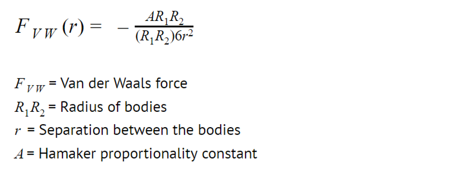
Van der Waals forces/London Dispersion Forces: These are the weak intermolecular electric forces that come into play between electrically neutral entities. In AFM, these forces act between the sample being examined and the cantilever's tip. A key characteristic of Van der Waals forces is their inverse proportionality to the distance separating the interacting bodies [5]. In the AFM setup, when the cantilever tip is near the sample surface, these attractive force-distance parameters tend to pull the tip towards the surface, causing a deflection of the AFM cantilever.
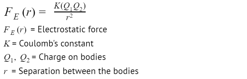
Electrostatic forces: These are the forces exerted between charged bodies. Depending on the charge, these forces can be either repulsive (between like charges) or attractive (between opposite charges) [6]. In AFM, as the cantilever tip is brought close to the sample surface, these electrostatic forces become significant. Initially, when the tip approaches the surface, Van der Waals forces dominate, drawing the tip closer and causing the cantilever to bend towards the surface. However, as the tip gets closer, electrostatic repulsive forces begin to overpower the attractive forces. This shift is partly because the tip cannot penetrate the surface of the sample. As a result, the cantilever, initially bending towards the sample, is now repelled away from it.
This interaction and the resultant change in the cantilever's deflection provide valuable information about the physical properties of the sample, such as its rigidity. Furthermore, AFM is not just limited to scanning and imaging; it can also measure the forces acting on the cantilever tip due to the sample. This capability allows for a more comprehensive analysis of the sample's surface properties, making AFM a versatile tool in material science and nanotechnology.
Construction of the Cantilever Tip/AFM Probe
The cantilever tip, an integral component of the Atomic Force Microscope (AFM), is a remarkably fine and acute point affixed to a slender, probe-like structure, referred to as the cantilever. This tip, notable for its precision and sharpness, is essential for the AFM's ability to conduct high-resolution surface scanning and accurate force measurements at the nanoscale.
On the opposite end of the cantilever, away from the sharp tip, resides a piezoelectric crystal. This crystal plays a pivotal role in the functionality of the AFM. It acts as a transducer, which means it has the capability to convert the mechanical movements of the cantilever into electrical signals. This conversion is critical for detecting and quantifying the subtle movements of the cantilever, which occur due to the interactive forces between the tip and the sample.
Moreover, the piezoelectric crystal is not limited to just one-way conversion. It also possesses the ability to transform electrical signals back into mechanical motion. This feature is crucial for the meticulous control over the positioning of the cantilever and its tip in relation to the sample's surface. By modulating the electrical input to the piezoelectric crystal, the position of the cantilever can be precisely adjusted, enabling the AFM to perform detailed and accurate scans of the sample's topography.
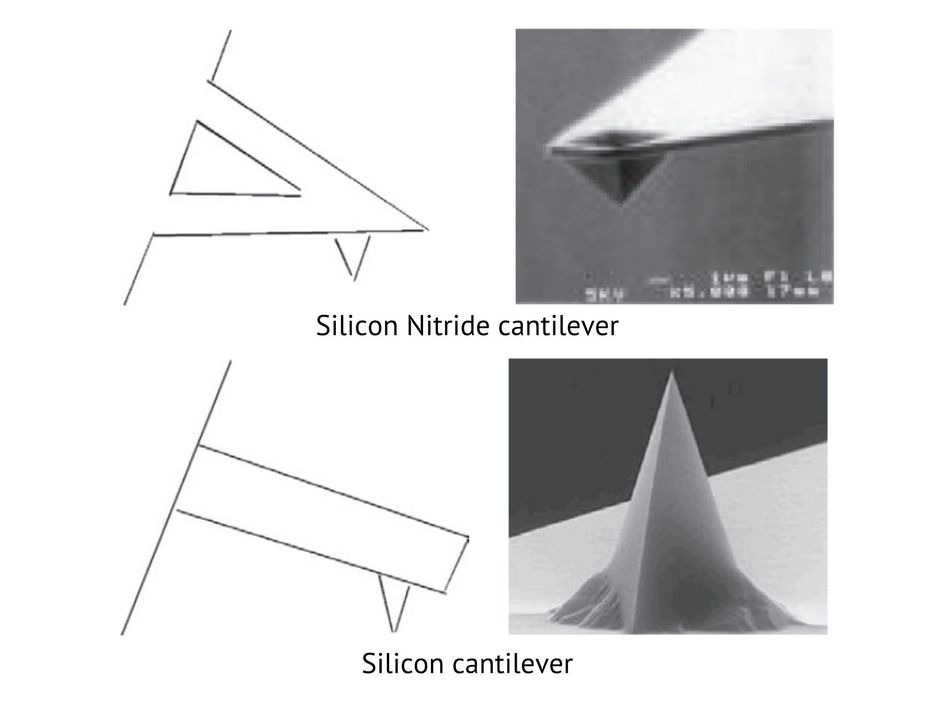
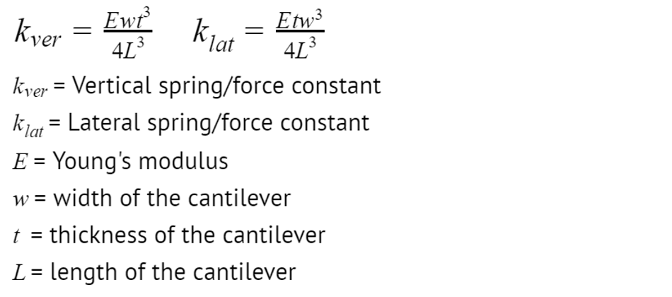
Documented through Scanning Electron Microscope (SEM) figure above, the cantilever tips' construction varies based on the sample's hardness. Silicon (Si) cantilevers are typically chosen for analyzing harder samples, while Silicon Nitride (Si3N4) is preferred for softer specimens. The selection of material hinges on the spring constant of the sample, which influences the cantilever's interaction with the sample's surface.
The design of the cantilever also involves meticulous calculations of its dimensions, ensuring that the required spring constants are met in both vertical and lateral directions. This consideration is vital for the accuracy of the AFM's measurements and imaging. The superior lateral resolution of AFM allows for the detailed visualization of surface features at the nanometer scale.
Here are the formulas used during the design of the cantilever:
In scenarios demanding heightened accuracy, the probe microscope tip undergoes further refinement processes such as electrochemical etching, ion milling, or attachment of a carbon nanotube. These enhancement techniques, while increasing the overall cost of the microscope, are crucial for obtaining high-quality scans. Inadequate selection of cantilever and tip materials could lead to compromised scan results, underscoring the importance of precise material choice and cantilever design in AFM technology [7].
Deflection Sensitivity Calibration/Spring Constant Calibration
Calibrating the spring constant of an Atomic Force Microscope's (AFM) cantilever is a critical process, foundational to its accurate functioning. This calibration adheres to Hooke's Law, which delineates a fundamental relationship among the applied force, the spring constant, and the deflection of the cantilever. Hooke's Law is mathematically represented as:
F=−kx
In this equation, F denotes the applied force, k represents the spring constant, and x indicates the cantilever's deflection. The negative sign is a conventional notation indicating the direction of the force relative to the displacement.
The calibration process involves fine-tuning the cantilever spring constant to ensure optimal sensitivity to the specific range of forces it is expected to encounter during measurements. This adjustment is essential for the AFM to detect and accurately measure the minute forces at play when the cantilever tip interacts with the sample surface. By precisely calibrating the spring constant, the AFM can reliably translate these interactions into meaningful data, crucial for the analysis of the sample's surface properties at the nanoscale.
Feedback mechanism
In AFM, ensuring consistent measurement accuracy necessitates maintaining the cantilever tip's distance from the sample within a specific range throughout the scanning process. The criticality of this distance control arises from two primary considerations:
High Separation Issue: If the gap between the tip and the sample is too large, the interaction force weakens significantly. In such cases, the force's signal strength diminishes, leading to a scenario where noise overshadows the actual signal, thereby impairing the accuracy of the measurements.
Low Separation Issue: Conversely, if the tip is too close to the sample, the exerted force becomes excessively strong. This increased force poses the risk of potential damage to either the sample or the instrument itself.
To address these challenges, AFM instruments incorporate a feedback loop control system. A Proportional Integral Derivative (PID) control scheme is commonly employed to constantly monitor and adjust the separation between the tip and the sample. This system operates as follows:
A predetermined reference value for the tip-sample separation or oscillating frequency is stored in the PID controller during the manufacturing and calibration phase of the device.
During operation, the real-time separation or oscillation frequency is measured and fed back to the PID controller. The controller then calculates and minimizes the difference between this current value and the preset reference point.
The transfer equation of a typical PID controller is given by:

The PID controller comprises three terms—Proportional (P), Integral (I), and Derivative (D)—each handling different aspects of the control process. The P and D terms primarily facilitate smooth movement over larger surfaces, while the I term is crucial for managing finer details in smaller areas. Optimal setting of these P, I, and D values is essential to minimize error in the feedback system. This system can be implemented using Operational Amplifiers (OpAmps) or digital circuits, depending on the design of the AFM.
The pivotal question then is: how is the relative position of the tip in relation to the sample altered during operation? The answer lies in the use of piezoelectric materials. These materials exhibit the unique property of expanding or contracting in response to applied electrical voltages. Substances like amorphous lead barium titanate (PdBaTiO3) are subjected to varying voltages, which in turn manipulate their expansion and contraction. This precise control of piezo-electric materials' dimensions enables the accurate movement of either the cantilever or the sample, crucial for maintaining the ideal separation distance during AFM operation.
AFM Modes
AFM employs a variety of modes to accommodate different types of samples and measurement objectives. These modes can be primarily divided into two broad categories:
Contact Mode/Static Mode AFM
In contact mode of operation, the cantilever's tip engages directly with the sample's surface, effectively being "dragged" along it. This mode is particularly advantageous for studying hard surfaces, offering high-resolution AFM observations greater than 50 nanometers (50 x 10-9 meters). The contact between the tip and the surface forms the basis of the data collected in this mode, as the tip's interaction with the surface's topography generates measurable deflections in the cantilever.
Static Force Mode: The static force mode in AFM focuses on measuring the cantilever's strain to deduce the surface structure of the sample. This mode is adept at analyzing hard surfaces, capturing the detailed topography through the cantilever's response to surface variations. However, it may not be suitable for sticky or soft samples, such as biomolecules, where the interaction between the tip and the sample could alter the sample's structure or result in the tip adhering to the sample.
Lateral Force Mode: In lateral force mode, the emphasis shifts from imaging to studying the mechanical properties of the sample's surface. This mode is particularly useful for measuring frictional and adhesive forces. As the cantilever's tip contacts the surface and moves across it, it encounters frictional resistance opposing its motion.
This frictional force causes the tip to incline slightly as it slides over the surface. Variations in the sample's frictional and adhesion alter the coefficient of friction, leading to changes in the tip's tilt angle.
As the tip traverses different areas of the sample, experiencing changes in the coefficient of friction, it undergoes corresponding alterations in orientation. When the tip moves over a surface area where the coefficient of friction returns to its baseline value, the tip reverts to its original position. This dynamic interaction between the tip and the sample's surface allows for detailed analysis of the surface's material properties, enhancing the understanding of its characteristics.
Dynamic Mode AFM
Dynamic modes of operation in AFM involve oscillating the cantilever's tip during measurements. This approach is designed to minimize or entirely avoid physical contact with the sample, ensuring a non-destructive interaction.
Dynamic Force Mode (Tapping Mode): This mode is widely used due to its effectiveness and minimal sample damage. The cantilever is set to resonate at a high frequency and is positioned close to the sample's surface. In tapping mode, the tip intermittently contacts the sample surface, allowing for detailed surface imaging while reducing the risk of damaging delicate samples.
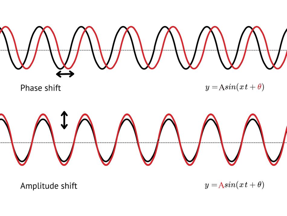
Phase Imaging Mode: In this dynamic mode, the tip oscillates at a fixed or resonant frequency over the sample's surface. Sample properties, such as adhesive forces, can impede the tip's immediate response to the input signal, resulting in a lag or delay. This delay causes a phase shift between the oscillation of the cantilever and the driving signal. Measuring this phase shift provides valuable information about the specific properties of the sample being examined.
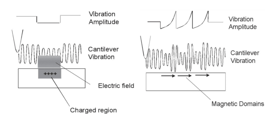
Field Mode: Field mode is an advanced AFM application used for measuring electromagnetic fields on a sample's surface. In this mode, the AFM tip is coated with either a conductive or magnetic material, depending on whether electric or magnetic properties are being measured. When this coated tip encounters electric or magnetic fields on the sample's surface, it experiences a force that affects both the tip and the cantilever. While this additional coating can slightly reduce the instrument's resolution, the extent of this effect depends on the coating's quality and thickness. In field mode, the amplitude of the tip's oscillation changes as it moves over regions with active electric or magnetic fields, with no direct contact between the tip and the sample. This method allows for the non-invasive measurement of a sample's electromagnetic properties.
Overall, dynamic modes in AFM offer a range of techniques for analyzing various properties of samples with minimal risk of altering or damaging the sample surface, making them invaluable in the study of sensitive materials and biological specimens.
Scanning methods for advanced imaging modes
The choice of scanning method varies based on the specific properties being measured and the characteristics of the sample. Two primary methods are employed for advanced imaging:
Single-Pass Method: This technique, also known as the constant height setup, maintains a fixed distance between the tip and the sample throughout the scanning process. It's designed for rapid data acquisition and is used for assessing either the surface properties or the electromagnetic field properties of the sample. In a single-pass scan, the probe traverses the sample's surface only once, hence the name. This method is particularly effective for quickly obtaining an overview of the sample's topography or field characteristics.
Dual-Pass Method: The dual-pass method is employed when both contact and non-contact forces need to be measured. As the name suggests, in this mode, the probe passes over the sample's surface twice during a single scan. The first pass is dedicated to mapping the surface topography, where the probe is in physical contact with the sample. The second pass then measures the non-contact forces, such as magnetic or electric fields, with the probe positioned at a predetermined distance above the surface. This dual-pass approach allows for a comprehensive analysis of the sample, capturing both its physical structure and the field properties in a single scanning session.
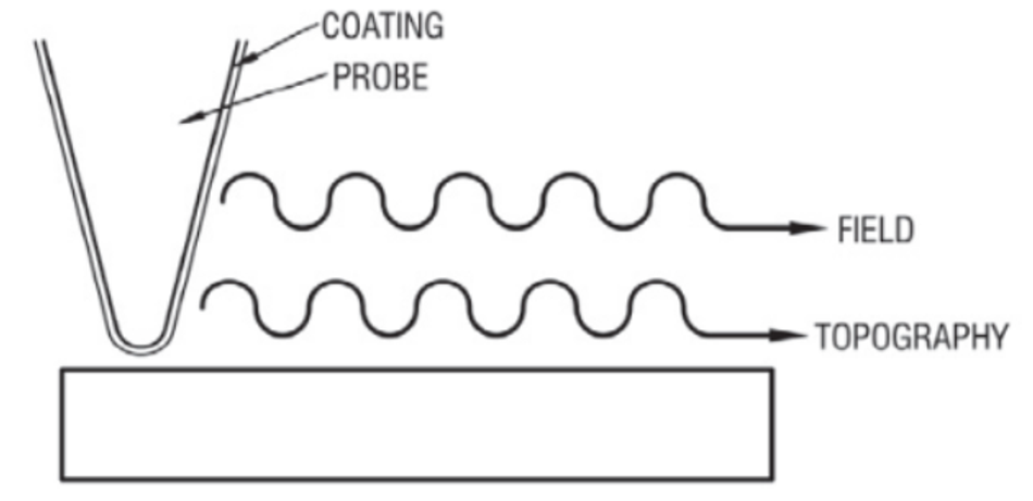
When the probe is in contact with the surface, the topography is measured; when it is at a fixed distance from the surface, it measures the field.
Atomic Force Microscopy Applications
AFM boasts a diverse range of applications, transcending the confines of any single field of study. This versatile technology finds utility in multiple disciplines, encompassing physical sciences, life sciences, electronics, and various branches of engineering [8].
Surface Analysis: AFM is extensively used to examine surface textures, defects, and coatings. It excels in providing high-resolution AFM images and detailed characterizations of various physical surface features.
Biological Studies: In the realm of life sciences, AFM is a powerful tool for observing cells, membranes, proteins and biomolecules within their natural environments. AFM can image live cells in their natural environment, providing crucial insights into cellular morphology and dynamics. Its ability to operate under physiological conditions makes it invaluable for studying biological samples in situ [9].
Microelectronics: The technology is adept at analyzing microelectronic circuits and components. AFM can be used for inspecting the surface topology and properties of semiconductor devices, ensuring quality control in the production of electronic components.
Energy Research: In the field of energy research, AFM plays a crucial role. It is used for studying materials used in energy storage, such as batteries, and energy generation, like photovoltaic cells. These investigations help in understanding and improving the efficiency and durability of these materials.
Tribology and Surface Chemistry: The microscope is instrumental in tribology for analyzing surface interactions, wear, and lubrication. In surface chemistry, it helps in understanding chemical properties and reactions at the surface level. It’s an indispensable tool for studying the nanomechanical properties of nanomaterials. The open architecture of AFM systems facilitates the integration of various spectroscopy methods enabling researchers to conduct comprehensive surface analyses, from studying chemical composition to observing molecular interactions.
Genetic Engineering and Medicine: AFM finds applications in genetic engineering, aiding in the manipulation and study of genetic material. In medicine, it is used for researching disease mechanisms and the development of new therapeutic techniques.
Overall, AFM's ability to provide detailed surface imaging and force measurement of nanoparticles at the nanoscale makes it an essential tool in a wide array of scientific and industrial applications, contributing significantly to advancements in research and technology [10].
Conclusion
AFM has revolutionized nanoscale surface study despite certain limitations, such as its relatively slow scanning speed and inability to directly analyze chemical properties. Nonetheless, its unparalleled ability to detail surface characteristics at the nanoscale makes it an invaluable tool in a range of fields, from product development and quality control in industries to advanced research and education in academic settings.
The evolution of microscopy, led by technologies like AFM, extends beyond traditional 2D imaging and visualization, integrating advanced computing to visualize objects and processes with remarkable clarity. While microscopy continues to advance, the enduring significance of optics in this field remains a constant, balancing between foundational principles and innovative advancements. This ensures that AFM and similar technologies will remain central to scientific and technological explorations in the future.
References
[1] Freundlich, M. M. (1963). Origin of the Electron Microscope. Science, 142(3589), 185–188. http://www.jstor.org/stable/1712183
[2] Abdullah, Avin & Mohammed, Azad. (2019). Scanning Electron Microscopy (SEM): A Review.
[3] Binnig, G, Quate, C, Gerber, C. "Atomic Force Microscope". Phys. Rev. Lett. 1986; 56:930–933
[4] Gerber, C., Lang, H. How the doors to the nanoworld were opened. Nature Nanotech 1, 3–5 (2006). https://doi.org/10.1038/nnano.2006.70
[5] Britannica, The Editors of Encyclopaedia. "Van der Waals forces". Encyclopedia Britannica, 16 Mar. 2016, https://www.britannica.com/science/van-der-Waals-forces. Accessed 6 October 2021
[6] Electric force [Internet], Khan Academy, Available from: https://www.khanacademy.org/science/electrical-engineering/ee-electrostatics/ee-electric-force-and-electric-field/a/ee-electric-force, [Accessed Oct 2021]
[7] Paul E. West, Introduction to Atomic Force Microscopy: Theory, Practice, Applications, Pacific Nanotechnology, 2006,2018
[8] Asylum Research - An Oxford Instruments Company. (2019, December 04). Applications of Atomic Force Microscopy (AFM) - A Guide. AZoNano. Retrieved on October 05, 2021, from https://www.azonano.com/article.aspx?ArticleID=5182
[9] Vahabi, S., Nazemi Salman, B., & Javanmard, A. (2013). Atomic force microscopy application in biological research: a review study. Iranian journal of medical sciences, 38(2), 76–83
[10] Robert W. Carpick and Miquel Salmeron, Scratching the Surface: Fundamental Investigations of Tribology with Atomic Force Microscopy, Chemical Reviews 1997 97 (4), 1163-1194, DOI: 10.1021/cr960068q
[11]Atomic force microscopy (AFM) [Internet], Available from: https://wiki.anton-paar.com/in-en/atomic-force-microscopy-afm/ [Accessed Oct 2021]
[12] Binnig G., Gerber C., Stoll E., Albrecht T.R., Quate C.F. (1993) Atomic Resolution with Atomic Force Microscope. In: Neddermeyer H. (eds) Scanning Tunneling Microscopy. Perspectives in Condensed Matter Physics (A Critical Reprint Series), vol 6. Springer, Dordrecht. https://doi.org/10.1007/978-94-011-1812-5_33
[13] Aliofkhazraei, M, Ali, N. "AFM Applications in Micro/Nanostructured Coatings". Comprehensive Materials Processing 2014; 7:191-241.
[14] Etzler, Frank. (2012). Atomic Force Microscopy for Characterization of Surfaces, Particles and their interactions
[15] Electron Microscope: What is it? [Internet], Available from: https://www.microscopemaster.com/electron-microscope.html [Accessed Oct 2021]