Bandgap Voltage Reference: Complete Guide for Analog Engineers
Master the Bandgap Voltage Reference — understand the physics, compare popular topologies, explore real-world applications, and choose the right IC for your analog design. A practical guide for engineers.

05 Jun, 2026. 20 minutes read

Key Takeaways
Core principle: A bandgap voltage reference adds a positive-temperature-coefficient (PTAT) term derived from the thermal voltage V_T = kT/q to a negative-temperature-coefficient (CTAT) base-emitter voltage V_BE of a bipolar transistor. Proper scaling yields a temperature-independent output around 1.23 V at room temperature [5].
Widlar, Brokaw, and Kuijk topologies: Classic bandgap references use two or three bipolar transistors and resistors to form PTAT and CTAT voltages. Widlar's design (1971) uses emitter-area ratios; Brokaw (1974) introduced a two-transistor cell with collector current sensing to eliminate base current errors, with the stabilized voltage appearing at a high-impedance node — making output scaling to voltages such as 2.5 V straightforward [6][1]; Kuijk (1974) uses a low-device-count BJT topology (two transistors and three resistors) that has been widely adapted for use with parasitic PNP devices available in standard CMOS processes [10].
Low-voltage and sub-1V designs: Modern CMOS bandgap references, such as the Banba architecture, convert PTAT and CTAT quantities to currents and sum them through a resistor, enabling operation from supplies below 1 V [2].
Curvature correction: First-order compensation cancels linear temperature drift, but higher-order terms remain; first-order-only designs are typically limited to around 20 ppm/°C over a 100 °C range. Exponential, quadratic, and piecewise-linear corrections reduce residual curvature [8].
Practical specifications: Monolithic bandgap references without curvature correction typically achieve temperature coefficients of 10 to 40 ppm/°C [4], while high-grade curvature-corrected devices reach sub-5 ppm/°C, with research-level implementations demonstrating below 1 ppm/°C drift [11] [4].
Trimming methods: Laser trimming, zener-zap, and digital trim allow calibration of resistor ratios to improve accuracy [4]. Each method trades off precision, cost, and in-package programmability.
Introduction
Precision voltage references are the unsung heroes of analog integrated circuits. They provide a stable reference voltage against which analog-to-digital converters, digital-to-analog converters, amplifiers, and sensors measure signals. Historically, discrete zener diodes served as voltage references, but their breakdown voltage exhibits strong temperature dependence and noise. Buried-Zener references improved noise and drift yet require high supply voltage and power. Bandgap references emerged in the mid1960s as the first monolithic solution that combined low voltage, low noise, and good temperature stability.
Robert Widlar, building on ideas from David Hilbiber, created a bandgap voltage reference using two transistors with different emitter areas and resistors. The circuit delivered approximately 1.25 V and achieved drift around ~20–50 ppm/°C untrimmed. [6]. Analog Devices fellow A. P. Brokaw later introduced a three-terminal bandgap reference that uses a negative feedback loop — implemented with an op-amp — to force equal currents through two bipolar transistors with different emitter areas, summing their ΔVBE and V_BE to produce a stable output. With trimming and curvature correction, implementations of this topology can reach roughly 5 ppm/°C ; the basic untrimmed cell typically exhibits closer to 20 ppm/°C.
Why Bandgap References Matter
Every analog circuit that measures, converts, or regulates something needs a stable voltage to compare against. That voltage is the reference — and if it drifts with temperature, everything downstream drifts with it. A 10 ppm/°C reference sounds precise, but across a −40 to 125 °C industrial range that is still a 1.65 mV shift on a 1.25 V output — enough to corrupt the least-significant bits of a 16-bit ADC.
Discrete zener diodes were the original solution, but uncompensated devices can drift by hundreds to over 1,000 ppm/°C. Temperature-compensated zener circuits close much of that gap, yet even trimmed designs rarely better ±10 to 100 ppm/°C without significant effort. Buried-zener references go further still — devices such as the AD586 achieve 2 ppm/°C on the best grade — but they demand a minimum 6 to 6.5 V supply, consume more power, and carry a higher price.
Bandgap references offer the best of both worlds. By summing two opposing temperature behaviors present in any bipolar transistor, they produce a reference voltage near 1.25 V that is anchored to silicon's own physics rather than to a carefully trimmed breakdown junction. The result is a reference that achieves low single-digit ppm/°C with curvature correction, operates from supplies as low as 1 V in modern low-voltage topologies, generates acceptably low noise for most applications, and fabricates directly in standard CMOS or bipolar processes without exotic materials or special structures. For the vast majority of precision analog ICs — ADCs, DACs, sensor front-ends, power management — the bandgap reference is the practical optimum.
What is a Bandgap Voltage Reference?
A bandgap voltage reference is a precision analog circuit that generates a stable, known voltage largely independent of temperature, supply voltage, and manufacturing process variation. It is one of the most fundamental building blocks in analog integrated circuit design — found inside virtually every ADC, DAC, sensor interface, power management IC, and data acquisition system made today.
The name comes from the energy bandgap of silicon — the fundamental physical property of the semiconductor material that determines the voltage at which the circuit naturally stabilizes. Because this voltage is set by silicon's atomic structure rather than by any external component, it is inherently stable and reproducible across chips and across time.
A bandgap reference works by combining two opposing temperature behaviors found in any bipolar transistor:
A base-emitter voltage (V_BE) that decreases with temperature (CTAT)
A thermal voltage (V_T = kT/q) that increases with temperature (PTAT)
When these two terms are summed in the correct proportion, their temperature drift cancels, leaving a stable output of approximately 1.25 V at room temperature — anchored to silicon's bandgap energy, which extrapolates to 1.205 V at absolute zero.
This combination of temperature stability, low supply-voltage requirement, low noise, and compatibility with standard CMOS fabrication processes makes the bandgap reference the dominant voltage-reference architecture in modern analog IC design.
The Physics of a Bandgap Voltage Reference
Thermal and Base-Emitter Voltages
The fundamental mechanism behind a bandgap reference is the opposing temperature dependence of two voltages. The base-emitter junction of a bipolar transistor (BJT) exhibits complementary-to-absolute-temperature (CTAT) behaviour. As temperature increases, the base-emitter voltage V_BE decreases at approximately 1.8 to −2 mV/°C [2]. The thermal voltage V_T = kT/q increases linearly with absolute temperature, providing a proportional-to-absolute-temperature (PTAT) voltage with a slope of approximately +0.086 mV/°C [2].
By generating a PTAT voltage proportional to V_T and summing it with a scaled CTAT voltage, a designer can achieve a temperature-independent output. The reference voltage extrapolated to absolute zero equals the silicon bandgap energy divided by the electron charge, approximately 1.2 V (commonly cited as 1.205 V in literature).
Summing CTAT and PTAT Terms
The simplest bandgap cell uses two bipolar transistors, Q1 and Q2, operating at different current densities. If Q2 has N times the emitter area of Q1 (or operates at N times the current), the difference in their base-emitter voltages ΔV_BE equals V_T · ln(N). This ΔV_BE has a positive temperature coefficient and thus acts as a PTAT voltage. A resistor network scales ΔV_BE and sums it with the CTAT V_BE of one transistor. By choosing the resistor ratio such that the positive and negative slopes cancel, the output becomes nearly independent of temperature.
When the scaled sum of ΔV_BE and V_BE is tuned so that the opposing temperature slopes cancel, the room-temperature output at which the temperature coefficient is minimized is approximately 1.25 V. The scaling factor is often tuned by design or trimming to achieve this cancellation across process corners.
First-Order Approximation
First-order analysis yields the reference voltage:
V_REF = V_BE(T₀) + m · V_T(T₀) · ln(N),
where m is a resistor ratio, T₀ is a nominal temperature (e.g., 300 K), and ln(N) is the natural logarithm of the area or current ratio. Setting dV_REF/dT = 0 and using dV_BE/dT ≈ –2 mV/°C and V_T ≈ 25.85 mV at 300 K yields m · ln(N) ≈ 17 to 23, giving V_REF ≈ 1.2 V.
Classic Bandgap Reference Topologies: Widlar, Brokaw, and Kuijk
Widlar Bandgap Reference
The first commercial bandgap reference was patented in 1971 by Robert J. Widlar. The design uses two NPN transistors operating at different current densities, established by an emitter area ratio, and a resistor network to sum the resulting PTAT and CTAT voltages. The PTAT voltage ΔV_BE appears across a resistor and is scaled by a resistor ratio before being added to the V_BE of one transistor:
V_O = V_BE + (R2 / R1) · ΔV_BE
Choosing the resistor ratio such that the opposing temperature slopes cancel yields an output of approximately 1.25 V at room temperature. Because the output node is directly connected to the resistor-transistor network without a buffer, the reference has relatively high output impedance and cannot drive significant load currents. Without curvature correction, first-order compensation limits temperature drift to around 20 ppm/°C over a 100 °C range.
Brokaw Bandgap Reference (1974)
Four years later, A. P. Brokaw published "A Simple Three-Terminal IC Bandgap Reference" in the IEEE Journal of Solid-State Circuits (December 1974). Brokaw's key innovation was a two-transistor cell that uses collector-current sensing to reduce errors caused by base-current variability — a problem present in earlier designs. A negative feedback loop, implemented with an op-amp, forces equal collector currents through the two transistors. Since one transistor has a larger emitter area, a ΔV_BE appears across a resistor, generating a PTAT voltage. The output is taken from the op-amp output, giving low output impedance and the ability to source or sink current:
V_OUT = V_BE + (R2 / R1) · V_T · ln(N)
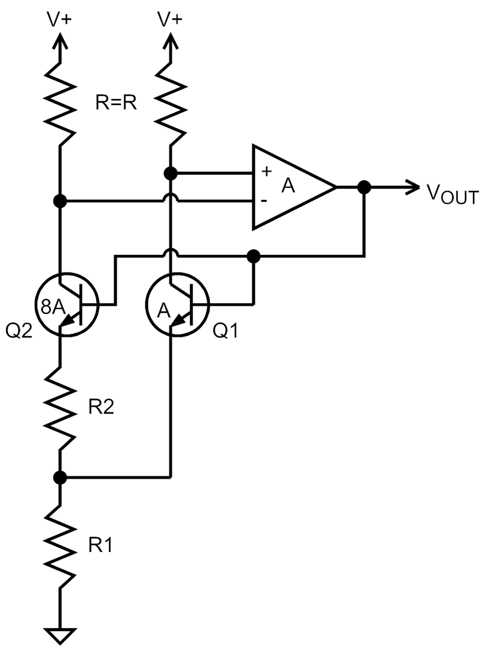
Brokaw bandgap voltage reference circuit
The 1974 monolithic implementation, trimmed over the military temperature range, achieved a temperature coefficient of 5 ppm/°C. The basic untrimmed cell typically exhibits closer to 20 ppm/°C. It is worth noting that in standard CMOS processes, which lack vertical NPN transistors, PNP substrate devices are commonly used in place of the NPN pair, with an op-amp implementing the current-forcing function [1].
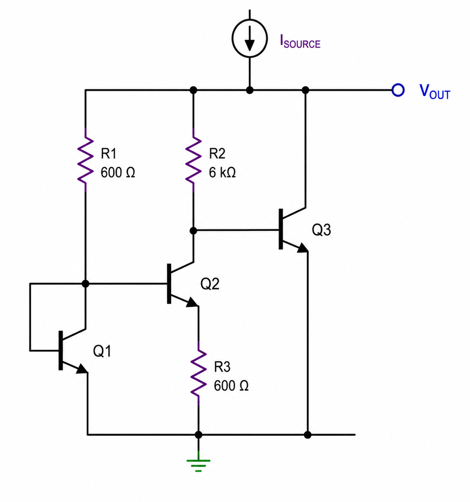
Kuijk Bandgap Reference (1973)
Karel E. Kuijk published his bandgap reference topology in 1973, predating Brokaw. The Kuijk cell uses two diode-connected BJTs and an operational amplifier. The reference voltage is the sum of a V_BE term (CTAT) and a scaled PTAT term derived from the voltage difference across two resistors carrying currents through the two BJTs:
V_REF = V_BE + V_T · (1 + R1/R3) · ln(IS1·R1 / IS2·R2)
The bipolar bandgap circuit proposed by Kujik.
The topology is well-suited to CMOS n-well processes because it naturally accommodates PNP substrate transistors, which are available without requiring deep n-well structures. In practice, common-centroid layout techniques are applied to the BJT pair to improve matching and reduce drift, though this is a layout practice rather than a defining feature of the topology itself [10].
CMOS Bandgap Reference Circuit
Traditional bandgap cells produce around 1.2 V, which exceeds the supply voltage in deep-submicron CMOS. In 1999, Banba and coworkers proposed a current-mode CMOS bandgap that generates PTAT and CTAT currents and sums them through a resistor to produce a lower reference voltage [2]. Banba's paper reports a 518 mV reference voltage with ±15 mV variation across 23 samples and temperature coefficients of a few tens of ppm/°C [2].
Sub-1V and Low-Voltage Bandgap Designs
Banba Architecture and Current-Mode Bandgap
Banba et al.'s 1999 design remains a benchmark for low-voltage references. The key equations are:
I_PTAT = ΔV_BE / R1, I_CTAT = V_BE / R2, V_REF = (I_PTAT + I_CTAT) · R3.
Selecting R1, R2, and R3 adjusts the PTAT/CTAT weighting and output voltage. Banba's measurements showed a reference voltage of 518 ± 15 mV over a temperature range of 27 to 125°C across 23 chips with a supply as low as 1.0 V [2].
Other Low-Voltage Techniques
Resistive subdivision: A conventional 1.2 V bandgap generates V_REF, which is then divided by a resistor network to produce lower voltages such as 0.6 V or 1.0 V. The noise and line regulation penalties of this approach are design-dependent — poorly implemented dividers can degrade PSRR at high frequencies and increase sensitivity to supply variation — and the approach typically consumes more quiescent power than a natively low-voltage topology.
Bootstrap references: Some designs use charge pumps or switched capacitors to boost internal voltages, allowing the use of conventional bandgap circuits while operating from sub-1V supplies. Switched-capacitor implementations have demonstrated improved supply rejection compared to current-mode sub-1V counterparts.
Sub-bandgap references: Newer research explores using the subthreshold characteristics of MOSFETs as temperature-compensated voltages, enabling supply voltages as low as 0.5 V and power consumption as low as 32 nW [12]. However, MOSFET threshold voltage has a larger process spread than BJT V_BE — process sensitivity without trimming can reach 2 to 3%, compared to 1 to 2% for well-designed BJT bandgap cells, and trimming or calibration is typically required to meet precision targets.
Curvature Correction Techniques for Bandgap Voltage References
First-order bandgap references cancel the linear temperature dependence of V_BE, but higher-order terms remain due to phenomena such as mobility variation and series resistance.
Exponential and Quadratic Correction
Using a diode-connected transistor biased at a different current generates a compensating term proportional to T·ln(T). By summing this with the original PTAT/CTAT combination, designers can cancel second-order terms. This technique can reduce drift by an order of magnitude — from the 20–100 ppm/°C range of first-order designs down to low single-digit ppm/°C, and high-order compensation has demonstrated below 1 ppm/°C in 0.18-µm CMOS [11].
Piecewise-Linear Correction
Rincon-Mora and Allen (1998) introduced a piecewise-linear curvature correction circuit using multiple PTAT current sources that turn on at different temperatures. Their implementation achieved a 0.595 V reference operating from a 1.1 V supply with only 14 µA current and 408 ppm/V line regulation [8]. Piecewise-linear segments improved the temperature coefficient beyond first-order compensation by cancelling curvature across the operating temperature range of the design.
Second-Order and Logarithmic Correction
Second-order compensation uses additional terms scaled to cancel the nonlinear temperature behaviour of V_BE. Rather than a V_T² term, the target nonlinearity is the T·ln(T) component of V_BE, which can be partially compensated by biasing transistors at different current densities or by using resistors with controlled temperature coefficients to introduce a correcting curvature. Including these terms reduces curvature and yields TCs below 1 ppm/°C in well-optimised designs. Exponential correction exploits the temperature dependence of the current gain β of bipolar transistors to generate a nonlinear compensating term that approximates the T·ln(T) behaviour in V_BE — this approach requires no additional compensation circuits beyond a size adjustment of a bias transistor in a conventional first-order design.
Practical Specifications and Performance Metrics
Temperature Coefficient (TC)
The temperature coefficient (TC) quantifies how much the reference voltage drifts per degree Celsius, expressed in ppm/°C. It is the primary specification engineers use to compare voltage references. Most datasheets use the box method — measuring the output at the temperature extremes and at room temperature, then expressing the worst-case deviation as a fraction of the nominal output divided by the temperature range — rather than a simple slope.
Monolithic bandgap references without curvature correction typically achieve 10 to 40 ppm/°C. With first-order correction, 2 to 10 ppm/°C is common. High-performance curvature-corrected devices reach 1 to 3 ppm/°C, and research-level implementations have demonstrated below 1 ppm/°C.
Initial Accuracy and Trim
Initial accuracy is the output voltage error at room temperature before any system-level calibration, expressed as a percentage of the nominal output. Untrimmed bandgap references typically have initial errors of ±0.5 to ±2 percent due to process variation. Laser-trimmed devices narrow this to ±0.02 to ±0.1 percent. High-end references such as the ADR4520 specify ±0.02 percent initial error alongside a TC as low as 0.8 ppm/°C, though achieving both simultaneously requires careful trimming and is reflected in the device's price tier.
Power Supply Rejection Ratio (PSRR)
PSRR measures how well the reference rejects noise and ripple on the supply rail, expressed in dB. It is strongly frequency-dependent — most bandgap references achieve 60 to 80 dB at DC and low frequencies, degrading to 20 to 40 dB at 1 MHz as the feedback loop bandwidth limits rejection [13].
Quoting PSRR without a frequency is therefore meaningless; always check the PSRR vs frequency curve in the datasheet. Devices like the ADR280 deliver around –80 dB PSRR at low frequencies. For applications with switching regulators on the supply, PSRR at 100 kHz to 1 MHz is the relevant figure, not the DC value
Dropout Voltage and Operating Range
Dropout voltage is the minimum difference between the supply voltage and the reference output required for correct operation. For bandgap references it typically ranges from 200 mV to 500 mV. The MAX6126 operates with as little as 200 mV of headroom, making it suitable for low-supply systems. Designers working near the dropout limit should account for supply ripple — a noisy supply that dips close to the dropout threshold will degrade both PSRR and TC performance [4].
Load and Line Regulation
Load regulation describes how much the output voltage changes with load current. A well-designed bandgap reference with an output buffer achieves output impedances below 1 Ω — the MAX6126, for example, specifies 0.025 Ω — keeping load-induced errors in the microvolt range for typical load currents. Line regulation, which measures output change per volt of supply change, is typically 5 to 50 µV/V for precision references. A decoupling capacitor at the output reduces transient droop during sudden load changes and improves high-frequency PSRR, but some references require a minimum capacitive load for stability — check the datasheet for any ESR or capacitance restrictions.
Output Noise
Bandgap reference noise has two components. Low-frequency noise (0.1 to 10 Hz) is dominated by 1/f noise and is typically quoted in µV peak-to-peak — the MAX6126 specifies 1.3 µVpp in this band. Broadband noise is quoted as a spectral density in nV/√Hz; buried-zener references generally outperform bandgap references here, with figures around 40 to 100 nV/√Hz versus 100 to 300 nV/√Hz for typical bandgap designs. For ADC reference applications, broadband noise integrated over the ADC bandwidth determines the noise floor, so the spectral density figure is more relevant than the 0.1–10 Hz figure [4].
Long-Term Stability
Long-term stability describes how much the reference output drifts over time at a fixed temperature, expressed in ppm over a given period (typically 1,000 hours). The MAX6126 specifies 20 ppm per 1,000 hours. To put this in context, a 20 ppm/1,000 h drift on a 2.048 V reference represents a 41 µV shift — enough to affect the least-significant bits of a 16-bit ADC. Buried-Zener references generally offer better long-term stability than bandgap designs, which is the primary reason they remain preferred in metrology and high-precision instrumentation despite their higher supply voltage requirement.
Start-Up Circuit
A bandgap reference has two stable operating points: the correct bias point and a zero-current state where all transistors are off. Without a start-up circuit, the cell can latch into the zero-current state at power-on and remain there indefinitely. The start-up circuit must source enough current at high temperature — where transistor gains are lower, and the main loop is slower to self-start — to push the circuit into the correct operating point, yet must switch off cleanly once the reference is running to avoid perturbing the output [13]. A poorly designed start-up circuit that does not fully disengage can degrade TC and noise performance.
Trimming and Calibration
Voltage reference accuracy is ultimately limited by process variation — even a well-designed bandgap cell will produce an output that differs from its nominal value by 0.5 to 2 percent across a production wafer. Trimming and calibration are the techniques used to correct this error, either at the wafer level, after packaging, or in the end system. The choice of method involves tradeoffs between precision, cost, timing in the production flow, and long-term stability.
Laser Trimming
Laser trimming uses a focused laser beam to vaporise sections of thin-film resistors on the chip, permanently increasing their resistance. By trimming resistors in the PTAT or CTAT scaling network, manufacturers adjust the output voltage and temperature coefficient to meet specifications. Because resistors can only be cut — not restored — laser trimming is a one-way, iterative process: the circuit is measured, a trim is applied, measured again, and the process repeats until the output is within tolerance.
Laser trimming is performed at the wafer level before dicing and packaging, which means the chip cannot be re-trimmed after assembly. This is its primary limitation.
A key subtlety is that laser trimming can adjust resistor ratios in two directions depending on circuit topology — cutting a series resistor increases resistance, while cutting parallel paths in a ladder network decreases the effective resistance. Designers must account for this when laying out the trim structure
Zener-Zap Trimming
Zener-zap trimming applies a controlled high-current pulse across a reverse-biased p-n junction, causing avalanche breakdown that permanently short-circuits the junction. By placing zener links in series with segments of a resistor ladder, manufacturers can selectively short out resistor sections, decreasing the effective resistance in discrete steps.
The key advantage over laser trimming is that zener-zap can be performed after packaging, since it requires only electrical access to dedicated trim pins rather than optical access to the die. This makes it possible to trim at the final test stage under realistic thermal and electrical conditions. Zener-zap trim stability over time is generally good but slightly inferior to laser-trimmed thin-film resistors, particularly under thermal cycling.
Digital Trimming (DigiTrim)
Digital trimming covers a family of techniques that store trim values in on-chip non-volatile memory — including one-time programmable (OTP) fuses, antifuses, and EEPROM cells — and use these values to select among digitally weighted current sources or resistor segments. The stored code adjusts the PTAT/CTAT weighting or output scaling to bring the reference within specification.
Digital trimming can be performed at any point in the production flow including after final assembly, since it requires only standard electrical test access.
DigiTrim, a trademarked implementation by Analog Devices (originally Linear Technology), is one well-known example of this approach and is used in several precision reference families.
The main concerns with digital trim are long-term retention of the non-volatile memory cells and the added circuit complexity of the DAC and memory interface.
Calibration Approaches
Trimming at a single temperature — typically 25°C — corrects the initial output voltage error but does not address TC errors or curvature. For the highest precision, two-point or multi-point calibration is used.
Selecting and Using a Bandgap Reference IC
Part Number | Type / V_REF | TC (max) | Initial Accuracy | Supply Range | I_Q | Notes |
Analog Devices ADR4520 | Series, 2.048–5.000 V | 2 ppm/°C [4] | ±0.02% | 3 V–15 V | 950 µA | High precision; low noise; ±10 mA; dropout 300 mV |
Texas Instruments REF5025 | Series, 2.5 V and 5 V | 2.5 ppm/°C [7] | ±0.025% | 3.25–18 V | ~1.2 mA | Low noise 0.5 µVpp/V; ±7 mA output; excellent PSRR |
TI REF30E | Series, 1.25–5 V | ~4 ppm/°C [7] | ±0.1% | V_OUT + 1 mV to 12 V | 25 µA | Ultra-low power; enhanced accuracy over standard REF30; dropout near zero unloaded |
Analog Devices ADR280 | Series, 1.200 V | 40 ppm/°C [4] | ±0.4% [4] | 2.4–5.5 V | 16 µA | Micropower; high PSRR; max load 100 µA without buffer; battery-powered sensors |
Maxim MAX6126 | Series, 2.048–5.000 V | 3 ppm/°C [4] | ±0.02% | 2.7–12.6 V | 380 µA | Low noise 1.3 µVpp; ±10 mA; dropout 200 mV |
Linear Technology LT1019 | Series, 2.5–10 V | 3 ppm/°C typ(5 ppm/°C max) [4] | ±0.05% | 4.5–30 V | 0.65 mA typ, 1.2 mA max | Curvature corrected; ±10 mA; 0.5 ppm/V line reg |
Linear Technology LT1009 | Shunt, , 2.50 V | 100 ppm/°C (standard grade; precision grade lower) [4] | ±0.2% | 2.7–36 V | 400 µA | Classic bandgap; adjustable via third terminal |
Analog Devices LM4040 | Shunt, 2.048–5 V | 100 ppm/°C [4] | ±0.1% | (V_REF+0.3 V)–40 V | — | Two-terminal; ideal for current sinks |
Selection Tips
For high-precision instrumentation (24-bit ADCs), choose references with TC ≤ 3 ppm/°C and low noise (ADR4520, MAX6126, REF5025). Note that for true 24-bit precision over a wide temperature range, even 1–2 ppm/°C TC can introduce measurable errors — evaluate the full error budget before selecting.
Battery-powered sensors require low quiescent current. Use micropower references like ADR280 (16 µA) or REF30E (25 µA), which may have slightly higher TC than premium precision references, though the REF30E achieves approximately 4 ppm/°C, which is competitive with many non-micropower devices.
Shunt references like the LM4040 are convenient for simple circuits but have higher TC and require a minimum operating current set by the external resistor network.
Evaluate PSRR and noise if the supply is noisy. Decouple per the datasheet recommendations — some references require a specific capacitance range for stability
Using Bandgap References
Decouple supply and output: Place 0.1 µF and 1 µF capacitors close to the reference to reduce noise and maintain stability.
Consider load current: Ensure the reference can source or sink the required current without exceeding dropout voltage.
Thermal environment: Avoid placing the reference near power transistors or hot spots on the PCB.
Layout: Use careful layout practices to minimize noise, parasitic effects, and mismatch.
Start-up behaviour: Verify the reference starts reliably at cold temperature and high supply ramp rates [4].
Applications of Bandgap Voltage References
Bandgap voltage references are used anywhere a circuit requires a stable and accurate reference voltage. Common applications include:
Analog-to-digital converters (ADCs), where the reference voltage directly affects measurement accuracy
Digital-to-analog converters (DACs) used in signal generation and control systems
Low-dropout regulators (LDOs) and power-management ICs
Sensor interfaces and instrumentation amplifiers
Battery-management systems and charging circuits
Microcontrollers, processors, and mixed-signal SoCs
Precision measurement equipment and industrial control systems
Modern CMOS bandgap reference circuits are especially important in portable electronics because they can operate from low supply voltages while maintaining good temperature stability and low power consumption.
Common Pitfalls and Layout Considerations
Resistor and Transistor Mismatch
Mismatches between resistors and transistor current densities cause errors in PTAT/CTAT scaling. Use precision resistor processes, lay out resistors in common-centroid patterns, and design ratio-matched devices close together.
Thermal Gradients and Packaging Stress
Temperature gradients across the die create local heating and mechanical stress, changing V_BE and resistances. Place the bandgap circuit away from power devices and digital logic. Use die-level thermal management by placing the bandgap away from high-dissipation nodes, and select low-stress packages or apply stress-compensation techniques to mitigate piezojunction effects.
Noise Coupling and PSRR
Place the reference near ground, shield sensitive nodes with guard rings, and separate analog and digital ground planes. Use decoupling capacitors and, if necessary, RC filters on the output.
Start-up Failures
Bandgap references may latch in a zero-current state without a start-up circuit [4]. Ensure the start-up circuit is robust across temperature and supply ramps.
Current Leakage and ESD Structures
Parasitic substrate currents, exacerbated by mechanical stress, can couple into the bandgap circuit and degrade accuracy. Use guard rings and proper substrate isolation.
CMOS Compatibility and BJT Implementation
In purely CMOS processes, bandgap references often use lateral PNP or vertical NPN transistors. These transistors may have lower gain, higher base resistance and more process variation than dedicated bipolar processes, so trimming becomes more important.
Conclusion
Bandgap voltage references are foundational building blocks in analog integrated circuits. By combining a CTAT base-emitter voltage with a PTAT thermal voltage, they produce a stable voltage near 1.25 V at room temperature, which extrapolates to the silicon bandgap energy of 1.205 V at absolute zero [5]. Classic topologies such as the Widlar, Brokaw and Kuijk references illustrate ingenious circuit techniques to implement this principle. Modern current-mode and sub-1V bandgaps extend the concept to deep-submicron CMOS [2], while curvature-correction techniques push temperature coefficients into the low ppm/°C range [8]. With careful layout, trimming and start-up design, bandgap references deliver reliable and accurate voltages for many years, though long-term drift due to mechanical stress in plastic packages remains a consideration for the most demanding applications.
FAQ
What is a bandgap voltage reference?
A bandgap voltage reference is a circuit that generates a constant voltage largely independent of temperature, supply and process variations. It combines the base-emitter voltage of a bipolar transistor (which decreases with temperature) with a scaled thermal voltage (which increases with temperature). When properly weighted, the temperature coefficients cancel, producing a stable voltage close to 1.205 V, the extrapolated energy bandgap of silicon [5]. Bandgap references are widely used in ADCs, DACs, regulators and sensor interfaces.
Why is a bandgap reference approximately 1.2 V?
At absolute zero temperature, the extrapolated base-emitter voltage of a silicon transistor equals the energy bandgap divided by the electron charge, about 1.205 V. To cancel the negative temperature coefficient of V_BE (~–2 mV/°C), a bandgap reference adds a PTAT voltage derived from the thermal voltage V_T (~+0.086 mV/°C). The sum of V_BE and an appropriately scaled PTAT voltage yields a temperature-independent voltage close to the bandgap value [2].
What is the difference between Widlar and Brokaw bandgap references?
Widlar's bandgap (1971) uses two bipolar transistors with different emitter areas and a simple resistor network to add the PTAT and CTAT voltages. It produces ~1.25 V but has high output impedance and limited load capability [6]. Brokaw's bandgap uses a negative feedback loop to force equal collector currents through two transistors, eliminating base-current errors. [1]. This three-terminal device offers low output impedance, allows output scaling to arbitrary voltages and achieves lower temperature coefficients
How does a CMOS bandgap reference work?
In CMOS processes, designers use lateral PNP or vertical NPN transistors within the analog module. Kuijk's topology uses PNP devices and an op-amp to generate the PTAT and CTAT terms [10]. For sub-1V supplies, current-mode bandgap references such as the Banba architecture generate PTAT and CTAT currents using MOSFET current mirrors operating in saturation . These currents are summed through a resistor to obtain a lower reference voltage (~0.5 V) [2].
What are PTAT and CTAT in bandgap references?
PTAT stands for proportional to absolute temperature. It refers to voltages or currents that increase linearly with temperature, such as the thermal voltage V_T = kT/q and the difference between base-emitter voltages of transistors operated at different current densities (ΔV_BE). CTAT stands for complementary to absolute temperature and refers to voltages that decrease with temperature, primarily V_BE. Bandgap references combine a PTAT term and a CTAT term with appropriate scaling [4].
Why use a bandgap reference instead of a Zener diode?
Zener diodes in breakdown have higher noise, larger temperature coefficients, and require higher operating current and voltage (typically over 5 V). Bandgap references operate from low supply voltages (under 5 V), provide lower noise, and can achieve TCs down to a few ppm/°C [4]. While buried-zener references offer even lower drift and noise, they demand higher voltage and consume more power.
What is the typical temperature coefficient of a bandgap reference?
Monolithic bandgap references exhibit temperature coefficients ranging from 10 to 40 ppm/°C without curvature correction, narrowing to 2 to 10 ppm/°C with first-order compensation [4]. High-precision devices with curvature correction achieve TCs of 1 to 3 ppm/°C [4]. Designers can further reduce drift through trimming and calibration.
How do trimming and calibration improve bandgap references?
Process variations cause mismatches in resistor ratios and transistor characteristics, leading to output voltage spread. Laser trimming cuts thin-film resistors to adjust the PTAT/CTAT ratio; zener-zap trimming shorts resistor segments via avalanche breakdown; digital trimming uses fusible links to program current sources or resistor arrays [4]. Two-point calibration further adjusts curvature for wide temperature ranges.
References
[1] A. P. Brokaw, "A simple three-terminal IC bandgap reference," IEEE Journal of Solid-State Circuits, vol. SC-9, no. 6, pp. 388–393, Dec. 1974. [Online]. Available: Link
[2] E. Banba, H. Shiga, M. Umezawa, T. Atsumi, K. Sakui, and M. Ueda, "A CMOS bandgap reference circuit with sub-1-V operation," IEEE Journal of Solid-State Circuits, vol. 34, no. 7, pp. 923–928, Jul. 1999. [Online]. Available: Link
[3] B. Razavi, "The bandgap reference (invited paper)," IEEE Solid-State Circuits Magazine, vol. 8, no. 3, pp. 3–22, Summer 2016. [Online]. Available: Link
[4] Analog Devices, "MT-087: Voltage references." [Online]. Available: Link
[5] Analog Devices, "Bandgap reference," in Analog Devices Wiki - University Courses. [Online]. Available: Link
[6] G. A. Rincon-Mora and P. E. Allen, "A 1.1-V current-mode and piecewise-linear curvature-corrected bandgap reference," IEEE Journal of Solid-State Circuits, vol. 33, no. 10, pp. 1551–1554, Oct. 1998. [Online]. Available: Link
[7] Texas Instruments, "REF5025 low-noise, very low drift, precision voltage reference datasheet." [Online]. Available: Link
[8] K. E. Kuijk, "A precision reference voltage source," IEEE Journal of Solid-State Circuits, vol. 8, no. 3, pp. 222–226, Jun. 1973. [Online]. Available: Link
[9] P. R. Gray, P. J. Hurst, S. H. Lewis, and R. G. Meyer, Analysis and Design of Analog Integrated Circuits, 5th ed. Hoboken, NJ: John Wiley & Sons, 2009. [Online]. Available: Link
[10] R. C. Dobkin and R. J. Widlar, "Monolithic voltage regulators," U.S. Patent 3,617,859, filed Mar. 23, 1970, and issued Nov. 2, 1971. [Online]. Available: Link
[11] S. Huang, Z. Tan, Y. Chae, and K. A. A. Makinwa, "A sub-1 ppm/°C bandgap voltage reference with high-order temperature compensation in 0.18-µm CMOS," IEEE Transactions on Circuits and Systems I, vol. 68, no. 3, pp. 1160–1170, Mar. 2021. [Online]. Available: Link
[12] A. Shrivastava, K. Craig, N. E. Roberts, D. D. Wentzloff, and B. H. Calhoun, "A 32 nW bandgap reference voltage operational from 0.5 V supply for ultra-low power systems," in Proc. IEEE Int. Solid-State Circuits Conf. (ISSCC), San Francisco, CA, Feb. 2015, pp. 94–95. [Online]. Available: Link
[13] B. Razavi, "The design of a low-voltage bandgap reference," IEEE Solid-State Circuits Magazine, vol. 13, no. 3, pp. 6–16, Summer 2021. [Online]. Available: Link
in this article
1. Key Takeaways2. Introduction3. What is a Bandgap Voltage Reference?4. The Physics of a Bandgap Voltage Reference5. Classic Bandgap Reference Topologies: Widlar, Brokaw, and Kuijk 6. Sub-1V and Low-Voltage Bandgap Designs7. Curvature Correction Techniques for Bandgap Voltage References 8. Practical Specifications and Performance Metrics9. Trimming and Calibration10. Selecting and Using a Bandgap Reference IC11. Applications of Bandgap Voltage References12. Common Pitfalls and Layout Considerations13. Conclusion14. FAQ15. References