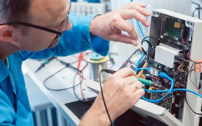
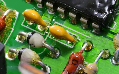
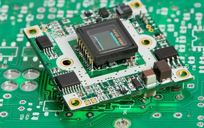
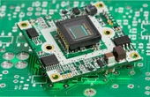
Be the first to know.
Get our Semiconductors  weekly email digest.

Semiconductors

report

The Guide to Understanding the Technologies Defining the Next Phase of Edge AI

PCB Trace Width Calculator

Glossary of Semiconductors Terms

Featured

The three themes are closely linked since QDs can be digitally printed as color conversation materials atop blue microLEDs to enable wide color gamut RGB uLED displays without requiring a separate transfer step for each color.. This is an important technology as it simplifies the manufacturing step for microLED and thus removing a major hinderence.

Engineers Wiki.

Most Asked Questions.

Comprehensive Guide

ORGANIZATIONS.

SHAPING THE INDUSTRY.

Nordic Semiconductor

Semiconductors

Nordic Semiconductor is a fabless semiconductor company specializing in wireless technology that powers the IoT.

181 Posts

MacroFab

EMS manufacturing

A better way to build electronics through a redefined experience, innovativ...

79 Posts

TechBlick

Electronics

TechBlick is a year round platform for onsite and online conferences, class...

65 Posts

OKdo

Appliances, Electrical, and Electronics Manufacturing

We’re OKdo, the global technology business from Electrocomponents Group. We...

37 Posts

Murata Electronics

Electrical and Electronics Manufacturing

Join the Innovators in Electronics.

37 Posts

TAGGED WITH pcb

Latest Posts

The three themes are closely linked since QDs can be digitally printed as color conversation materials atop blue microLEDs to enable wide color gamut RGB uLED displays without requiring a separate transfer step for each color.. This is an important technology as it simplifies the manufacturing step for microLED and thus removing a major hinderence.

PCB layers are the copper layers within a printed circuit board, laminated between or onto layers of conductive material. These layers are stacked to enhance the functionality of electronic devices. This article explores the concept of PCB layering, the various types of layers, and their benefits.

PCB Layers: Everything You Need to Know

Canadian researchers have discovered that they can stick hydrogel plasters to the skin very effectively using ultrasound. Outi Supponen has now explained the underlying mechanism: imploding bubbles that form within the adhesive located between the plaster and the skin anchor the one on the other.

Strong adhesion thanks to cavitation bubbles

As NASA prepares to send astronauts back to the Moon to live and explore, capabilities for space-based manufacturing of sensors, circuits, and other electronics will become increasingly critical. Recent microgravity flights have helped to advance cutting-edge methods for 3D printing of electronics

Microgravity Testing Advances Space-Based Printing of Electronics