Rendering PCBs Part 3 - Final steps
In this tutorial series it is all about the procedure of creating realistic renders from 3D models of PCBs in Blender. In the third (and last) part of this tutorial series, we will take a look at different steps that will lead to a better render result.
17 May, 2022. 4 minutes read
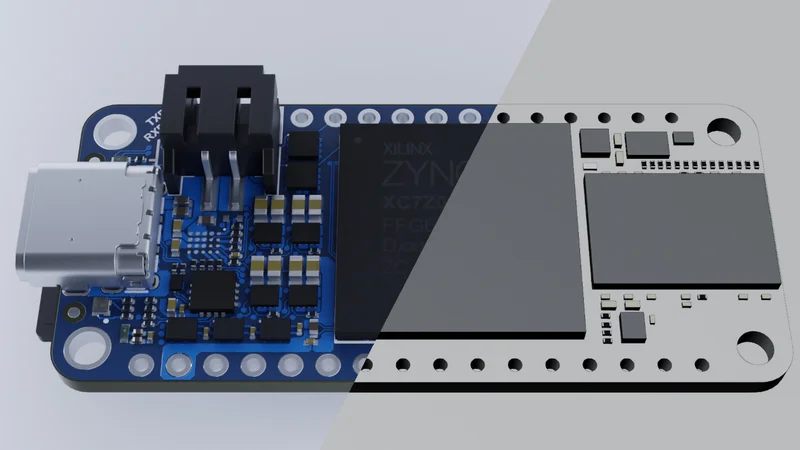
3D render of a PCB in Blender
On GitHub we provide a sample project. There you can download the blender file, which contains a complete setup with models, corresponding textures and shader settings.
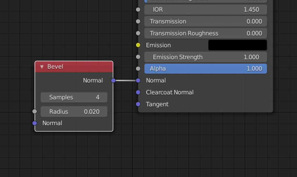
Bevel
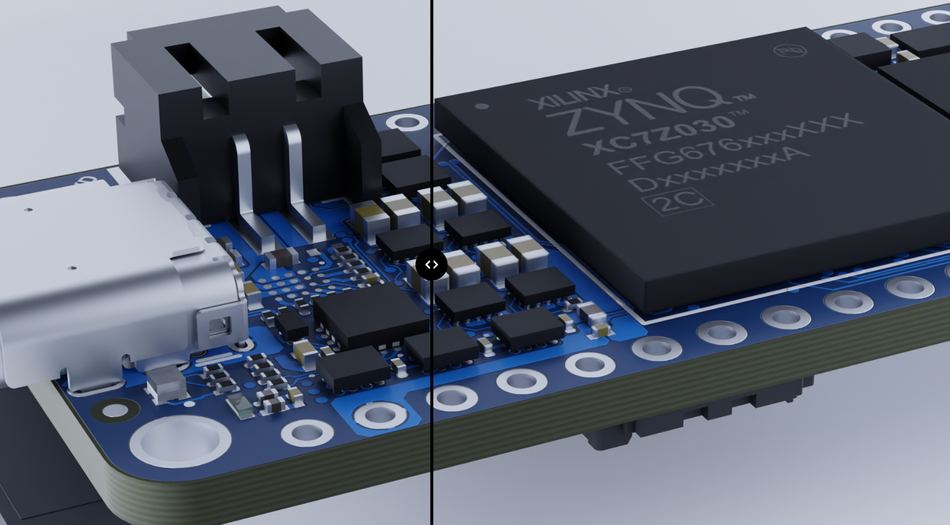
Most SMD components have a very simple geometry: they are straight boxes. Due to the perfect shape, renders often look unrealistic. For example, the JST connector of the Zynq-Feather has many sharp edges. In reality, the edges of connectors, IC packages or SMD components are more or less rounded because of inaccuracies and imperfect conditions during manufacturing.
With the help of a Bevel node, such rounded corners can easily be added to a material without having to change the geometry of a single or multiple objects. For this purpose, the node can be connected to the Normal input of a Shader node. The Radius can be used to influence the curvature. Generally small Radius values should be chosen for IC packages, because they usually have sharp corners. On the other hand, the solder contacts of SMD resistors, for example, are more rounded. In this case, larger values should be chosen. The following figure shows how a Bevel node can be configured in the Shader Editor.
At first glance, a difference is hardly noticeable. To get a better impression of the effect, take a look at the following illustration. There, two renders are laid on top of each other, one with and one without bevel. The image segments can be moved using the slider on our blog.
Using Bevel nodes was suggested by one of our Twitter followers. He mentioned it in one of his videos: youtube.com/watch?v=7ratnf0rIVU
Labels
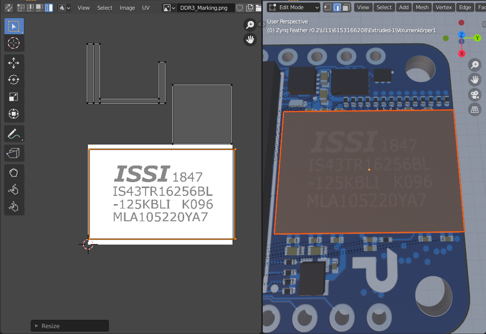
IC packages often have a label. It shows a product number, the name of the manufacturer or something similar. The next step is to see how such a label on a component can be implemented in Blender. For this, a texture is needed that contains the labeling as a black and white image. The labels are often shown in the data sheets of the components. They can be extracted from the PDF file of the data sheet as a screenshot or with the help of an image editing program. A UV Map must then be set up to project the texture onto the top of the IC package. All other faces should be placed outside of the image. To ensure that the label is not present on the other faces, the Extension attribute of the Image Texture node in the Shader Editor must be set to Extended (the default value is Repeat).
In the example of the Zynq-Feather a label is to be added to a RAM IC. The following screenshot shows how the UV Map was configured.
After the UV map has been set up correctly, the material of the component must be adjusted. Since ICs are often assigned the same materials during export, a copy of the material must first be created. This way, the subsequent changes will only apply to the selected part.
In the production of ICs, the markings are often applied to the packaging surface by a laser. By using a laser, the lettering is slightly brighter than the otherwise black packaging and less rough. This can be taken into account by controlling the 'Base Color' and the 'Roughness' of the material with the previously set up texture. For the Base Color a Mix node can be used, which mixes the black color of the case with the dark brown color of the marking. The Roughness can be controlled using the Map Range node. This maps the values of the texture from 0.0 (black) to 1.0 (white) to the range of values from 0.4 (rather smooth) to 0.8 (rough).
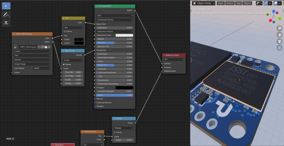
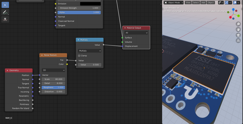
For close-ups it is also worth to add a Displacement to the ICs material. To create bumps in the surface, a Noise Texture can be used. The necessary nodes are shown in the following figure.
Denoising
The last thing that should be considered is the final result: the rendered image. In the Cycles mode, the rendered image is quite noisy. Depending on the number of samples , the noise is stronger or weaker. With a large number of samples the noise decreases, but the time for rendering increases. Even with a very high amount of samples, the noise is still noticeable. Hence, denoising should be applied to the render.
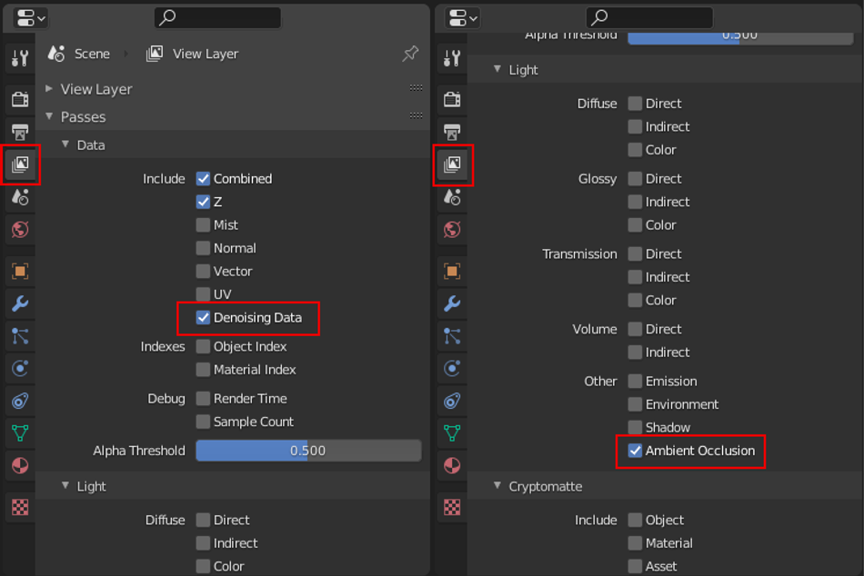
To set up denoising, the checkbox Denoising Data must be selected in the View Layer Properties in the Properties window under Passes. Another visual improvement can be achieved by using Ambient Occlusion, which can be activated in the same process (see screenshot).
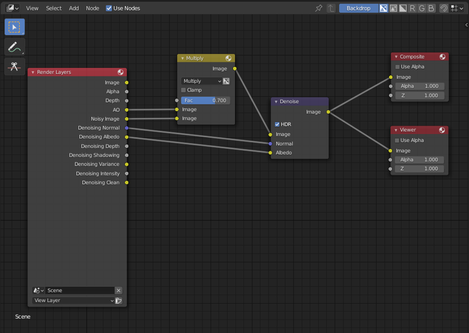
Finally, the activated render layers need to be considered in the Compositor in order to apply Denoising and Ambient Occlusion to the render result. The settings in the Compositor are shown in the screenshot below.
Conclusion
The PCB model has now been enhanced with additional details by adding labels to ICs and rounding materials to make them look more realistic. Also, the noise in the final render has been fixed. This is the end of the tutorial series about rendering PCBs in Blender.
The team of PCB Arts hopes you will have a lot of fun creating your own renders!