Enabling IoT Hardware Innovation with PCB Cloud Manufacturing Services
OEMs can focus on innovation and stay competitive by leveraging cloud manufacturing services.

02 Jun, 2022. 7 minutes read
Introduction
New manufacturing architectures are needed to meet the demand of the growing Internet of Things (IoT) market. This article discusses how PCB cloud manufacturing supports and enables IoT hardware development.
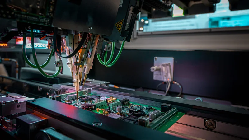
PCBs are at the center of the IoT devices, enabling transducers, processors, antennas, and other components that are part of the device to exchange power and data in the form of electricity effectively. PCB design for IoT products is more challenging than other electronic circuits as it often requires meeting tighter size constraints, stricter standards, and higher performance requirements.
These challenges pose a risk to IoT hardware innovation. However, a new method of design and manufacturing, known as PCB cloud manufacturing, is pushing back against these obstacles, and making space for IoT Hardware innovation.
PCB Design and Manufacturing Challenges for IoT Products
Some of the factors that make the PCB design and manufacturing process for IoT products complicated and potentially hinder innovation include:
Tighter size constraints
The trend for smaller, lighter products is not abating, so every millimeter of a PCB is crucial. As board real estate decreases, designers must look to emerging approaches such as rigid-flex and high-density interconnect (HDI) PCBs. Designing for tighter size constraints also demands expertise in planning optimized layout and component selection.
Unique PCB shapes
IoT devices come in all shapes and sizes, so PCBs may not always be able to be designed in their traditional rectangular shape. Designing an unusually shaped PCB with curves or cutouts requires good collaboration between the mechanical and electronics design teams to meet such constraints. Manufacturing oddly shaped PCBs may also be more expensive, requiring other design concessions.
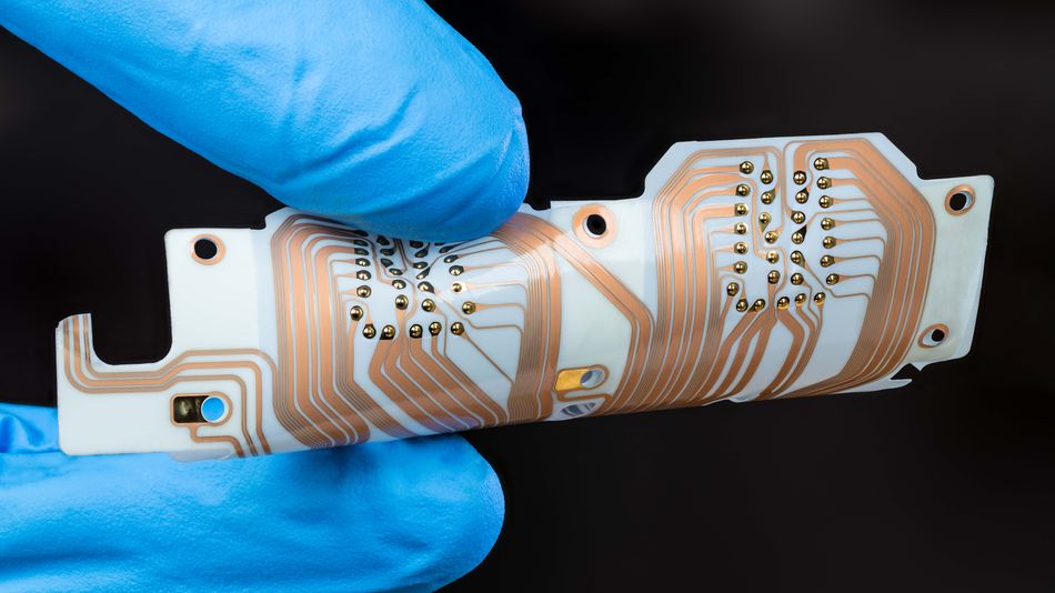
Variety of board materials
A rapidly emerging market of IoT is flexible wearables. The PCB may need to be made on flexible materials for these products, adding further design and cost restraints.
Power utilization and thermal constraints
As IoT devices are generally 'always on' and communicating with the network, designing low-power systems to ensure practical battery life is essential. In addition to being power-efficient, these products must also have a proper heat dissipation mechanism. These factors have placed a new emphasis on analyzing power integrity and optimizing power consumption during the design phase of PCBs. To build products that meet these complex constraints, additional time may need to be spent during the design phase adding pressure to design team resources.
High-pressure innovation demands
Further challenges are faced by IoT hardware teams by the enormous pressures of the cycles of innovation. Rapid technological advancements combined with increased user demand for new products means enterprises are under enormous pressure to reduce time to market. This pressure is further increased by global supply, demand, inventory management, and logistics issues.
Cloud Manufacturing Services Enable IoT Hardware Innovation
Digitizing just the PCB manufacturing process is not enough to deliver a momentum of innovation in the IoT space. Improvements are required across the design and development lifecycle, including data collection and application, analytics, and resource allocation.
The complex process of designing and manufacturing PCBs has been significantly enhanced by the advent of PCB cloud manufacturing services. PCB cloud manufacturing takes the dispersed and chaotic manufacturing process and streamlines it using tools such as Artificial Intelligence (AI) and cloud computing to offer enterprises manufacturing as a service (MaaS). The benefits of PCB cloud manufacturing services are broad but have a potent impact on contributing to IoT hardware innovation.
The following section outlines how PCB cloud manufacturing addresses the challenges above and contributes to industry innovation.
Optimizing Designs for Reliability and Performance
The lifecycle of an IoT product begins with development; this is where the product's core functionalities are set, and desired features defined. Crucial to this stage are Design For Manufacturability (DFM) checks – these checks surface potential design issues early prior to manufacturing. Cloud manufacturing platforms provide tools to assist in the process within their interface – meaning design teams can get assurance from potential manufacturers in a single process that will later involve the complete ordering of products.
DFM checks not only adds a layer of critical quality assurance and design support, but they can also identify component choices within the design that are more susceptible to supply chain issues. Designing for resilience within current constraints is essential for innovation to continue. This service offered by cloud manufacturing platforms offers a solution to design challenges such as tight layout and board and material selection to ensure that the PCB will fulfill the requirements of its application.
Data-Driven Control of the Manufacturing Process
PCB cloud manufacturing services offer a service-based approach instead of a product-based approach to production by setting up dynamic collaborations with service providers to carry out the various manufacturing tasks. PCB cloud manufacturing services give hardware enterprises a new realm of control over their manufacturing processes.
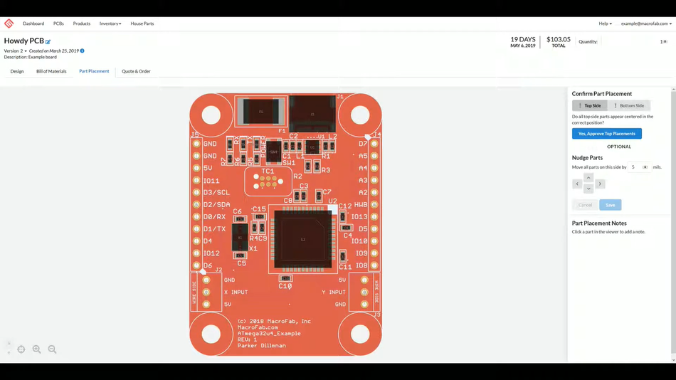
Generally, a cloud manufacturing service platform offers a centralized dashboard through which its customers manage the whole product lifecycle. Quotes and requests are placed via a single-entry point for orders of all scales from prototypes to mass production. This places the power of knowledge in the hands of innovators who can monitor orders, review processes, and scale to scale production up or down without penalties. In some instances – where cloud manufacturing platforms and software companies have teamed up - designers can place an order to produce their PCB without ever leaving their design environment. This lightens a considerable responsibility for hardware enterprises managing their manufacturing - freeing up time and staff resources to focus on innovation. Cloud manufacturing services can essentially become an external manufacturing expert allowing companies to leverage the expertise of their service providers, assisting them to design, test, and manufacture innovative products.
Source: Macrofab
Strict Quality Assurance for Defect-Free Products
All IoT products must also undergo rigorous testing to make sure the components used in the manufacturing process meet strict performance standards. The key to this quality assurance is unit testing. This occurs through a process where before the product is manufactured, a few modules are picked for quality assurance. This ensures that the component batches are genuine and working correctly. Further, quality assurance teams also perform functional and integration tests to ensure the end product is free from defects. The products are either deployed in the working environment or sent back for redevelopment based on the test results. The working environment is where the end-users get their hands on the product and share precious feedback.
PCB cloud manufacturing supports innovation at this stage of the lifecycle through their detailed data collection of this process. Analytic and visualization tools offered by PCB cloud manufacturing enable design teams to streamline the design process and shorten the time to market for future products. This kind of data can be the difference between product success and failure in an increasingly competitive industry.
Delivering continuous improvements
Once the product makes it through the testing phase, it is packed and delivered to the end-user, however, the life cycle of IoT products is a continuous process and require OEMs to revise the hardware and software as per the latest demands.
Hardware revisions are challenging to carry out owing to the complex manufacturing process. The time taken to complete an updated product can be stretched by searching for an available vendor to fulfill the new requirements. In such a scenario, having a cloud manufacturing service to assist with the supporting tasks can save the efforts and the hassle of overhauling the existing manufacturing process.
In the working environment and throughout the manufacturing process, enhancements are made as per the feedback to improve the board's functionality and user experience. At any point, if required, it is possible to go back to the planning board and begin the development of a particular module or a set of modules requiring improvements.
Conclusion
In summary, PCB cloud manufacturing significantly contributes to innovation in IoT hardware by addressing common PCB design and manufacturing challenges. Further, PCB cloud manufacturing frees up hardware enterprises to invest in innovation by reducing a significant portion of the risk and resources required to manufacture, assemble and test IoT products.
By offering end-to-end production, assembly, and testing agreements, PCB cloud manufacturing reduces the complexity of project management and ensures feedback on product development can be addressed quickly within a closed-loop environment. Without dealing with the complexity of manufacturing and supporting tasks, IoT hardware teams can instead collaborate with cloud manufacturing and focus on design, marketing, and growth, ensuring continued innovation.
PCB cloud manufacturing brings manufacturing resources and manufacturing services together to offer faster time to market, lower costs and effective project management that enables enterprises to focus on innovation.
About the Sponsor: MacroFab
MacroFab is an electronics manufacturing digital platform that provides production options throughout North America. MacroFab aims to make it faster and easier to bring new electronic products to market through its software-driven approach to electronics manufacturing.

References
[1] Alternative Sourcing: Risks and Strategies for Today's EMS Market, Macrofab, [Online], Available from: https://macrofab.com/documents/alternative-sourcing-risks-strategies-ems-market/
[2] Choose the Optimal Contract Manufacturer for New Product Prototyping, Macrofab, [Online] Available from: https://macrofab.com/documents/choose-optimal-contract-manufacturer-product-prototyping/