FPGA vs ASIC: Key Differences, Costs, and How to Choose
This guide delves into FPGA vs ASIC, providing a decision framework, cost-at-volume analysis, and modern examples to help you pick the right technology for your next project.

08 Jul, 2026. 13 minutes read
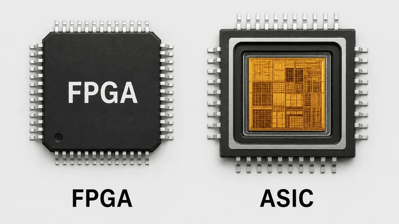
FPGA, ASIC
Key Takeaways
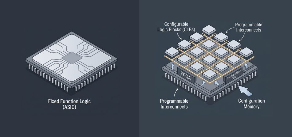
Different Architectures: ASICs are custom-designed chips optimized for a single application, while FPGAs are reprogrammable devices with arrays of logic blocks and interconnects. This fundamental architectural difference drives all other trade-offs.
Performance and Power: ASICs deliver higher performance and lower power consumption because they are purpose-built, whereas FPGAs incur overhead from their configurable fabric. Advances like Versal HBM series by AMD integrate high-bandwidth memory to mitigate bottlenecks.
Cost and Break-Even: ASIC development incurs high non-recurring engineering (NRE) costs, but per-unit prices drop below $1 in volume. FPGAs have lower NRE and faster time-to-market, but higher unit prices. The economic crossover typically lies between 5 k and 50 k units, depending on complexity and process node.
Design Flexibility: FPGAs offer rapid prototyping and field upgradability, making them ideal for evolving standards, low-volume production and customizable products. ASICs are fixed once taped out, so any change requires a new mask set and additional NRE.
Choosing the Right Chip: Use FPGAs when you need quick iteration, low- to medium-volume, or field updates. Opt for ASICs for high-volume, mature designs where performance, power efficiency, security and unit cost are paramount.
Introduction
Choosing between programmable logic and custom silicon is a critical decision in modern electronic product design. The FPGA vs ASIC comparison helps engineers evaluate flexibility, performance, development cost, power efficiency, and long-term production goals before committing to a hardware architecture.
FPGAs provide reconfigurable logic, faster prototyping, and lower upfront costs, making them suitable for evolving designs, low-volume products, and applications that require post-deployment updates. ASICs, on the other hand, are custom-built chips optimized for high performance, low power consumption, compact size, and large-scale manufacturing efficiency.
Understanding FPGA vs ASIC trade-offs is essential because the best choice depends on technical requirements, budget, time-to-market, and expected production volume. This article explains FPGA vs ASIC differences in cost, design flow, performance, and use cases. By the end, the FPGA vs ASIC decision should be clearer for engineers, product teams, and decision-makers.
What are FPGAs?
Definition and Architecture
Field-Programmable Gate Arrays (FPGAs) are integrated circuits whose logic functions and interconnects can be programmed after manufacturing.
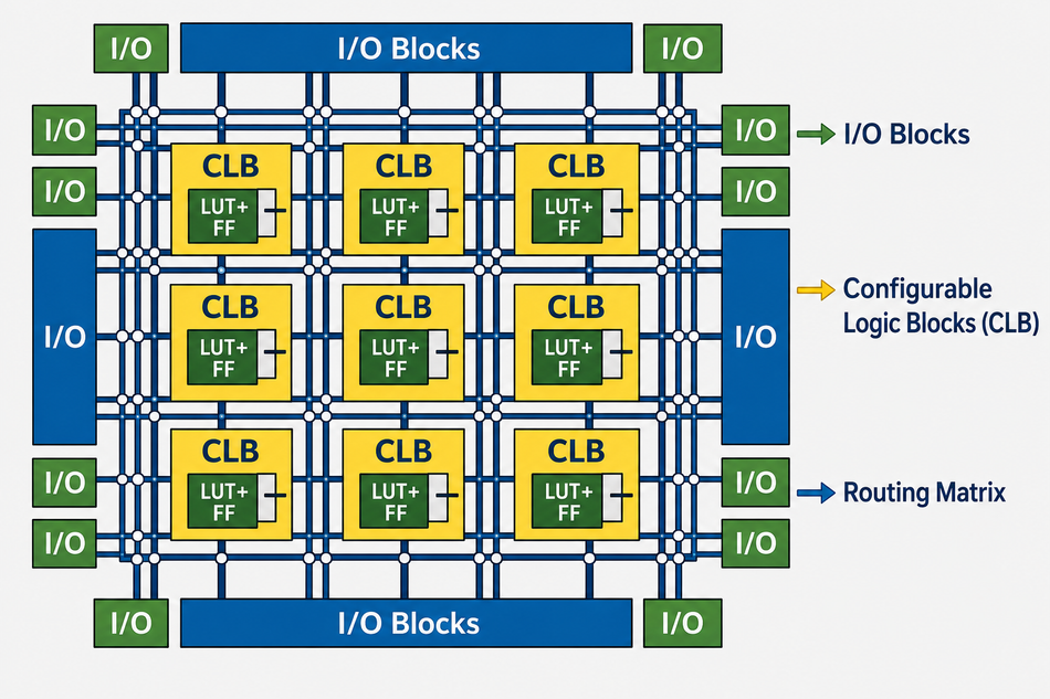
Typical FPGA consists of configurable logic blocks (CLBs) implementing look-up tables (LUTs) and flip-flops, programmable interconnects that link CLBs, dedicated I/O resources, on-chip memory (block RAM), and sometimes DSP slices or AI engines. Configuration is performed by loading a bitstream generated from a hardware description language (HDL) such as VHDL or Verilog. Because the logic and routing are programmable, a single FPGA can implement anything from simple logic to complex signal processing algorithms.
Design Flow
The FPGA design process begins with system specification, where requirements such as throughput, latency, power and cost are defined. During design entry, engineers express the circuit in HDL or using high-level synthesis. The synthesis step maps the HDL description into a netlist of FPGA primitives (LUTs, flip-flops, DSP blocks). The place and route assigns these primitives to specific locations and generates routing for interconnects, optimizing for timing and area. Then, verification includes simulation, timing analysis and in-circuit tests. Finally, a bitstream is generated and loaded onto the FPGA. Unlike ASICs, this process can be repeated to refine the design or fix bugs without new hardware. [1]
Modern FPGA Families
The last few years have seen rapid innovation in programmable logic. AMD - Versal HBM adaptive SoCs integrate stacked high-bandwidth memory in-package. In-package HBM delivers up to 8× the memory bandwidth at 63 % lower power than external DDR5 and offers 820 GB/s of bandwidth with 32 GB of capacity. Versal devices also include scalar (ARM), adaptable (FPGA fabric) and DSP engines, with SerDes bandwidth up to 5.6 Tb/s. This architecture supports networking, data-center and aerospace workloads.
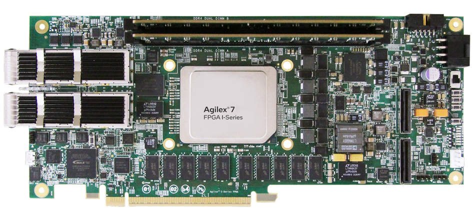
Intel - Agilex 7 I-series devices use chiplets called R-tiles to integrate hardware support for PCIe Gen5 and CXL 2.0, providing cutting-edge memory and interconnect features. The mid-range Agilex 5 E-series emphasizes cost-effectiveness and lower power for embedded edge applications. Agilex devices incorporate AI tensor blocks borrowed from the Stratix 10 NX FPGA for low-precision AI inference and embed a dual-core Arm Cortex-A76 + Cortex-A55 processor system to accelerate software integration. [5]
Lattice Semiconductor targets ultra-low-power applications. The CrossLink-NX family, built on the Nexus platform, consumes up to 75 % less power than similar FPGAs and supports standby currents under 70 µA. Devices are available in packages as small as 4 mm × 4 mm and include hardened MIPI and PCIe interfaces, making them suitable for IoT, vision and automotive systems. The broader look at a programmable spectrum (including CPLDs and microcontrollers) is covered in our CPLD vs FPGA and FPGA vs Microcontroller guides.
Recommended Reading: What Is an FPGA? Complete Guide to Field Programmable Gate Arrays for Engineers
What are ASICs?
Definition and Design Flow
Application-Specific Integrated Circuit (ASIC) is a chip tailored to perform a specific function. Once FPGAs use prefabricated logic blocks, ASICs are created by laying out transistors and interconnects to precisely implement a design. [2]
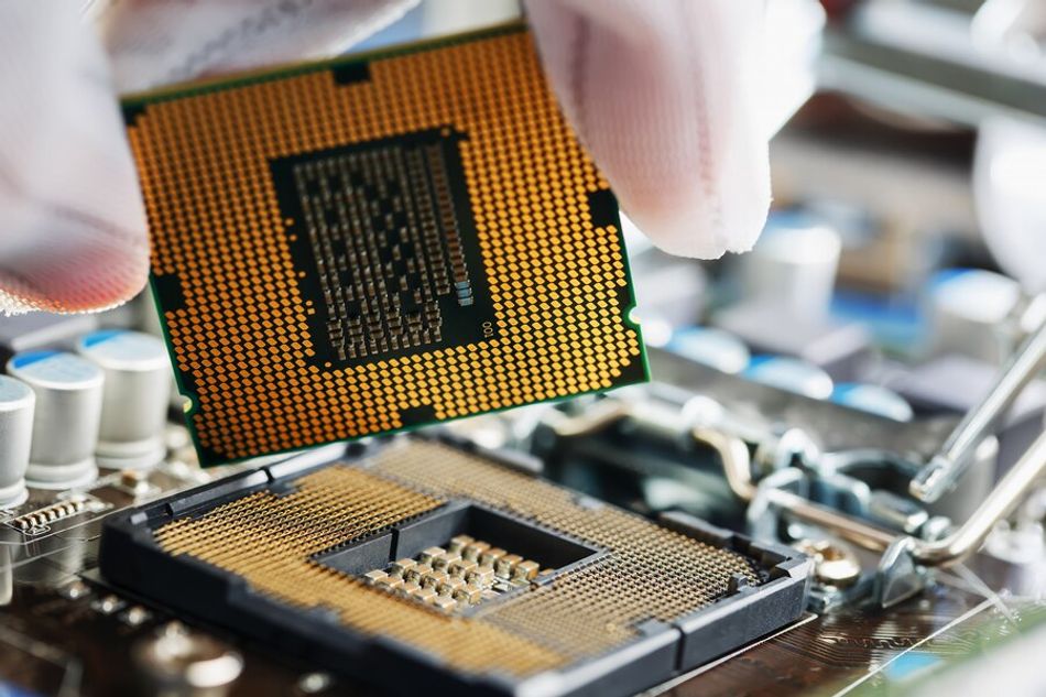
The design flow begins with system specification, followed by high-level architecture, logic synthesis, floorplanning, placement, routing, and verification. Once verified, the layout is turned into photolithography masks for fabrication. Fabrication involves many steps (mask creation, wafer fabrication, dicing and packaging) and is expensive and time-consuming. The functionality of the chip is fixed after fabrication.
Advantages
High Performance: Custom datapaths allow ASICs to achieve much higher clock speeds and throughput than equivalent FPGA implementations. Modern AI accelerators illustrate this: Google - TPU v6e (Trillium) packs 32 GB of high-bandwidth memory per chip and achieves around 918 TFLOPS of BF16 throughput.
Low Power: Eliminating configurability reduces switching activity and capacitance. ASICs therefore consume significantly less power than FPGAs.
Small Form Factor: Tailored layouts remove unused logic, enabling compact packages ideal for mobile and wearable devices.
Low Unit Cost at Scale: Once NRE is amortized, per-chip cost drops dramatically, often below a dollar for simple designs.
IP Protection: Proprietary algorithms are hard-wired, making them difficult to reverse-engineer.
Disadvantages
High Upfront Cost: NRE expenses cover design tools, verification, mask sets and fabrication, often $2 M-$15 M+.
Long Development Time: Design and mask creation can take months or years.
Inflexibility: Functionality is fixed after tape-out; redesigning requires a new mask set.
Obsolescence Risk: Rapid technological change can render a fixed design outdated before the product's end-of-life.
Modern ASIC Examples
The AI boom has driven a renaissance in custom chips:
Google TPU v6e/Trillium: Each TPU v6e chip includes 32 GB of HBM; the interchip interconnect (ICI) bandwidth is doubled versus the previous generation, and per-chip BF16 throughput is ~918 TFLOPS.
AWS Trainium2: Trainium2-powered Trn2 instances offer 30-40 % better price performance than GPU-based EC2 instances. A single Trn2 instance combines 16 Trainium2 chips to provide 20.8 petaflops of compute, and Trn2 UltraServers interconnect 64 chips for 83.2 petaflops. AWS and Anthropic are building an EC2 UltraCluster using hundreds of thousands of these chips.
Groq LPU: This Language Processing Unit (LPU) is a purpose-built AI inference chip that delivers up to 10× greater energy efficiency than GPUs. Its programmable assembly-line architecture and on-chip memory allow deterministic, high-throughput inference.
Tesla Dojo D1: D1 chip, part of the Dojo supercomputer, uses a 7 nm process and delivers 362 TFLOPS of BF16 performance; 25 chips form a tile (~=9 PFLOPS) and 120 tiles make a rack with over 1 exaflop of compute for training autonomous-driving models.
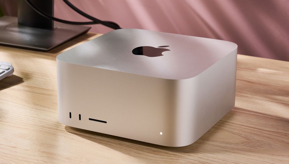
Apple M3 Ultra: This dual-die SoC uses Apple - UltraFusion packaging to link two M3 Max dies via over 10,000 high-speed interconnections; the resulting chip integrates 184 billion transistors. It features a 32-core CPU, up to 80-core GPU, over 800 GB/s of memory bandwidth, and supports up to 512 GB of unified memory. Apple claims up to 2× faster performance than the M2 Ultra while maintaining industry-leading power efficiency. [8]
These examples show how ASICs push performance and efficiency beyond what general-purpose silicon can offer. They also illustrate the high stakes: each chip represents tens of millions of dollars in development but enables products like cloud AI services, autonomous vehicles and high-end desktops.
Recommended Reading: What is an ASIC: A Comprehensive Guide to Understanding Application-Specific Integrated Circuits
Head-to-Head Comparison
Performance
Custom ASICs typically deliver higher performance than FPGAs because the logic and interconnects are optimized for a single task. Dedicated hardware can run at higher frequencies and handle more operations per cycle. For instance, TPU v6e by Google reaches roughly 918 TFLOPS of BF16 throughput per chip, orders of magnitude higher than typical FPGA designs. [3] FPGAs, however, have narrowed the gap by integrating DSP blocks and AI engines, as seen in Versal HBM devices by AMD, which combine scalar, adaptable and DSP engines for up to 5.6 Tb/s of SerDes bandwidth.
Power Consumption
ASICs consume less power because unnecessary gates and routing are eliminated. The energy per computation is lower, making them ideal for battery-powered or thermally constrained systems. The reprogrammable fabric in FPGA introduces capacitance and leakage, increasing power. Vendors address this with low-power families: CrossLink-NX by Lattice uses the Nexus platform to achieve up to 75 % lower power than comparable FPGAs and includes a standby mode drawing <70 µA. [6]
Cost: NRE and Unit Price
The economic trade-off hinges on the relationship between NRE costs and per-unit prices. According to industry-wide cost analysis:
FPGAs: NRE typically ranges from $25 K to $600 K (design, tools, IP licensing, verification). Because devices are off-the-shelf, there is no mask cost. Per-unit prices range from $5 to over $5 K depending on size, family and features.
ASICs: NRE can vary from $2 M to over $15 M for advanced nodes. Mask sets alone may cost several million dollars. However, per-unit prices can drop below $1 for simple designs and scale with die size and process technology.
The break-even volume (where total cost of ownership for an ASIC equals that of an FPGA) usually falls between 5 k and 50 k units. Factors like device complexity, node selection, FPGA discounts, team efficiency and product lifetime shift the crossover point. For small runs and prototypes, FPGAs are more economical because there is no large NRE. ASICs amortize NRE and yield a lower per-unit cost, at high volumes.
Design Flexibility and Field Upgradability
FPGAs excel at flexibility. You can reprogram the device to fix bugs, support new standards or repurpose hardware without manufacturing new silicon. This enables rapid prototyping, proof-of-concept demonstrations and iterative product development. Partial reconfiguration even allows updating a portion of the design while the rest continues running. ASICs are inflexible by comparison: modifications require a new design and mask set, incurring additional NRE and months of delay.
Time-to-Market
Development schedules also differ. FPGAs bypass the fabrication step entirely; once synthesis and place-and-route are complete, the bitstream can be downloaded to hardware. Many projects can go from concept to hardware in weeks, accelerating learning and market entry. ASIC projects must complete the full design flow, verification and fabrication, often taking 12-24 months. For products where early market presence is critical, FPGAs offer a significant advantage.
Security and IP Protection
ASICs provide stronger intellectual-property protection because the design is hard-wired. Reverse-engineering a custom chip is difficult and expensive. FPGAs store configuration in memory or flash; unauthorized access to bitstreams or configuration interfaces can expose proprietary algorithms. Designers can mitigate this through encryption and secure boot, but ASICs remain the more secure option by default.
Recommended Reading: Wafer Backgrinding: An In-Depth Guide to Semiconductor Manufacturing
Cost-at-Volume Analysis and Break-Even Curves
FPGAs typically have lower upfront expenses because there is no mask generation, fabrication setup, or tape out. The design and development may range from $1.0 × 10⁴ to $3.0 × 10⁵, while EDA tools, IP licensing, simulations, and verification can add further cost depending on design complexity. Overall FPGA non-recurring engineering costs often fall between $2.5 × 10⁴ and $6.0 × 10⁵, with unit prices ranging from a few dollars to several thousand dollars per device.
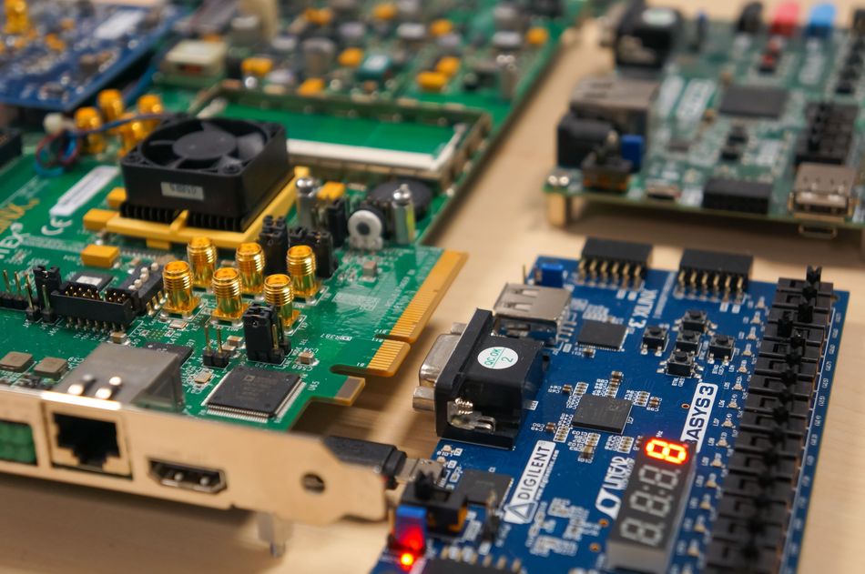
ASICs follow a very different cost structure. Their design flow includes system specification, RTL development, verification, IP integration, physical design, mask sets, fabrication setup, and post-silicon validation. Resultantly, ASIC NRE costs commonly range from $2.0 × 10⁶ to $1.5 × 10⁷ or more, especially at advanced semiconductor nodes. However, once in mass production, ASIC unit cost can fall below $1 for small, high-volume chips, or range higher depending on die size, yield, packaging, and process technology.
The break-even volume is the point where total ASIC cost equals total FPGA cost:
NRE (ASIC) + Unit Cost (ASIC) × N = NRE (FPGA) + Unit Cost (FPGA) × N
For example, consider an ASIC with $5.0 × 10⁶ NRE and a $3 unit cost, compared with an FPGA design requiring $2.0 × 10⁵ NRE and a $30 unit cost. The break-even volume is:
N = (5.0 × 10⁶ − 2.0 × 10⁵) / (30 − 3) ≈ 1.78 × 10⁵ units
Below roughly 1.78 × 10⁵ units, the FPGA remains more economical. Beyond that point, the ASIC becomes more cost-effective because its lower unit cost offsets the higher upfront investment. In real projects, the break-even point may occur much earlier, often between 5.0 × 10³ and 5.0 × 10⁴ units, especially when replacing expensive mid-range or high-end FPGAs in high-volume production.
Decision Framework: Which Should You Choose?
Choosing between an FPGA and an ASIC depends on design maturity, production volume, performance targets, power efficiency, and how much flexibility the final product requires. In many real-world systems, the decision is not always binary.
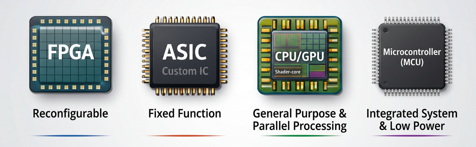
FPGAs are often used during early development, rapid prototyping, and validation, while ASICs are later adopted for high-volume production when the system specification becomes stable and cost optimization becomes critical.
Rapid Prototyping and Proof-of-Concept
For rapid prototyping, algorithm validation, or proof-of-concept development, an FPGA is usually the better choice. Its reconfigurable architecture allows engineers to test logic, digital signal processing functions, image processing pipelines, and embedded systems without waiting for semiconductor fabrication. Because there is no tape out or large non-recurring engineering cost, development cycles are shorter and design changes can be implemented quickly.
Low-Volume Production
For low-volume production, typically below 5.0 × 10³ units, FPGAs are often more practical. Although their unit cost is higher, the overall project cost remains manageable because the design avoids multi-million-dollar NRE costs, mask sets, and a complex ASIC design flow. This makes FPGAs suitable for industrial systems, specialized telecommunications equipment, research platforms, and products with uncertain demand.
Moderate Volume with Evolving Standards
For moderate production volumes, typically between 5.0 × 10³ and 5.0 × 10⁴ units, the decision depends on complexity, product lifetime, and expected design changes. If standards, interfaces, or customer requirements may evolve, an FPGA or hybrid approach is often preferred. Reconfigurable logic, configurable logic blocks, and programmable interconnects allow field updates, making FPGAs valuable in telecommunications, automotive platforms, and data center applications where flexibility matters.
High-Volume and Stable Specifications
For high-volume production above 5.0 × 10⁴ units, an ASIC is usually more cost-effective when the design is stable. ASICs amortize non-recurring engineering costs over large volumes and deliver lower unit cost, better power efficiency, smaller area, and higher clock frequencies. This makes them suitable for smartphones, consumer electronics, wearable devices, microprocessors, system-on-chip designs, and other mass-production semiconductor products.
AI, Cloud, and Edge Applications
For AI training at cloud scale, ASICs are generally preferred because dedicated accelerators can deliver higher throughput and energy efficiency than general-purpose programmable devices. However, for AI inference, edge-AI, and low-latency workloads, the choice may depend on the application. Specialized ASICs can provide deterministic latency, while advanced FPGAs can offer adaptable acceleration, high memory bandwidth, and flexibility for changing models or algorithms.
Ultra-Low-Power Edge and IoT Devices
For ultra-low-power edge devices, battery-powered devices, and compact IoT systems, the decision depends on power budget and production scale. Low-power FPGA families can be effective when reconfigurability is required, especially during early product development or specialized deployment. However, ASICs usually provide superior energy efficiency for mature, high-volume wearable, automotive, and consumer electronics applications.
Aerospace, Defense, and Reliability-Critical Systems
For aerospace, defense, and radiation-sensitive applications, both technologies may be used. Radiation-hardened ASICs provide strong reliability, predictable behavior, and long-term stability. Radiation-tolerant FPGAs, however, are useful when reconfigurable functionality, mission updates, or adaptable system behavior is required. The final choice depends on reliability targets, qualification requirements, environmental conditions, and the need for post-deployment changes.
Recommended Reading: CPLD vs FPGA: Key Differences and How to Choose
Modern Landscape (2025-2026)
The line between FPGAs and ASICs continues to blur. Systems on Chip (SoCs) now integrate both hardwired cores and programmable logic.
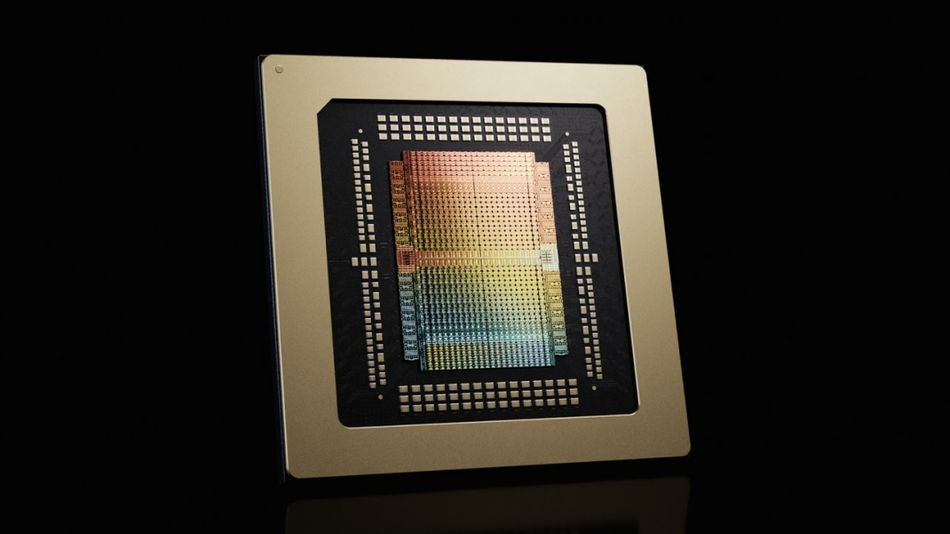
Engineers should be aware of the latest offerings:
Adaptive SoCs (FPGA-ASIC Hybrids): AMD - Versal adaptive SoCs combine scalar processors, adaptable FPGA fabric and DSP engines with high-bandwidth memory. [4] These devices function as mini-systems capable of running software and accelerating hardware tasks. They are used in data-center networking, radar, test and measurement and aerospace.
Hard IP inside FPGAs: Intel - Agilex family embeds hard PCIe Gen5/CXL tiles, AI tensor blocks and hardened processors. This reduces the performance gap while retaining flexibility.
Cloud AI Accelerators: Google - Trillium (TPU v6e) offers extreme compute density with 32 GB HBM and 918 TFLOPS. AWS - Trainium2 EC2 instances deliver 20.8 PFLOPS per instance and 30-40 % better price performance than GPU instances. [7]
Specialized Inference Chips: Groq - LPU achieves deterministic throughput and up to 10× energy efficiency vs GPUs. These chips illustrate how targeted architectures out-perform general-purpose GPUs and highlight when a custom ASIC pays off.
Custom SoCs for Consumer Devices: Apple - M3 Ultra sets a benchmark for desktop computers with 32-core CPU, 80-core GPU and 512 GB unified memory. It's an example of a custom ASIC optimized for a broad range of workloads within a single package. To understand how such chips are designed, see our guide on custom SoC design.
Recommended Reading: FPGA Boards: Hardware Architecture, Toolchains, and Development Platforms
Conclusion
Both FPGAs and ASICs are indispensable in modern electronics. ASICs deliver unmatched performance, low power consumption and low per-unit cost when amortized across large volumes. They underpin high-performance computing, AI accelerators and custom consumer SoCs. FPGAs, with their reprogrammability and rapid time-to-market, shine in prototyping, low-volume production, evolving standards and ultra-low-power applications.
The choice depends on the performance targets, power budget, production volume, design flexibility requirements and schedule of your application. Use FPGAs for agility and exploration; switch to ASICs for volume production and energy-efficient, high-performance designs. Hybrid solutions and adaptive SoCs blur the boundary, offering a mix of flexibility and specialization. By understanding the trade-offs and consulting the decision framework above, you can select the optimal platform for your next project.
Frequently Asked Questions
Q. Is an FPGA or ASIC cheaper?
A. FPGAs have lower NRE costs but higher per-unit prices, making them cost-effective at low volumes. ASICs require expensive semiconductor design and fabrication, but each microchip becomes much cheaper during high-volume production.
Q. Can an FPGA replace an ASIC?
A. FPGA can replace an ASIC in prototyping, testing, and low-volume products. However, ASICs are usually better for mature products that need lower power, smaller size, higher speed, and optimized analog or mixed-signal integration.
Q. Why are ASICs faster than FPGAs?
A. ASICs are faster because their circuits are custom-built for one function, with optimized datapaths and minimal routing overhead. FPGAs rely on configurable logic and programmable interconnects, which add capacitance, delay, and power consumption.
Q. Are FPGAs or ASICs used in AI?
A. Both are widely used in AI. ASICs power large-scale training accelerators, while advanced FPGAs support AI inference, image processing, and adaptable acceleration. FPGAs are especially useful when algorithms evolve or low-latency updates are needed.
Q. What is the difference between a programmable logic device (CPLD) and an FPGA?
A. CPLDs are simpler programmable logic devices used for glue logic, control tasks, and small designs. FPGAs provide far more logic, memory, routing, and digital signal processing resources for complex embedded systems and high-performance applications.
Q. Can I prototype on an FPGA and then migrate to an ASIC?
A. Yes. Many teams use FPGA prototypes to validate architecture, run simulations, and refine the system specification before ASIC development. Once the design is stable, engineers can move toward tape out and mass production.
Q. Are there security differences between FPGAs and ASICs?
A. Yes. ASICs hard-wire functionality, making reverse engineering more difficult. SRAM-based FPGAs store configuration data externally or internally at startup, so encryption and secure boot are important. Flash memory FPGAs can offer stronger non-volatile configuration security.
References
[1] Infineon. ASIC Solutions for a Wide Range of Applications [Cited 2026 July 07]; Available at: Link
[2] ACM. Comparison and Application of FPGA and ASIC in Digital System Design [Cited 2026 July 07]; Available at: Link
[3] Utmel. FPGA vs ASIC: Comprehensive Comparison Guide [Cited 2026 July 07]; Available at: Link
[4] AMD/Xilinx. AMD Versal™ HBM Series [Cited 2026 July 07]; Available at: Link
[5] EEJournal. Intel Heats Up and Expands its Agilex FPGA Family [Cited 2026 July 07]; Available at: Link
[6] Lattice Semiconductor. CrossLink-NX: FPGA for Embedded Vision Processing [Cited 2026 July 07]; Available at: Link
[7] Spheron Network. "Google TPU Trillium v6 vs NVIDIA B200: LLM Inference Cost and Migration Guide [Cited 2026 July 07]; Available at: Link
[8] Apple. Apple Reveals M3 Ultra, Taking Apple Silicon to a New Extreme [Cited 2026 July 07]; Available at: Link