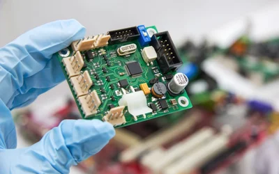
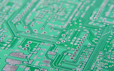
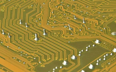
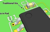
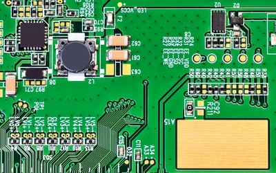
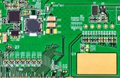
Advancements in power storage devices, Micro Electro Mechanical Systems (MEMS), Gallium Nitride (GaN) semiconductors, etc. are key to achieving carbon neutrality in various industries.
It is hard to think of a profession facing a more trying set of circumstances than farming. Climate change has brought higher temperatures and lower winter rainfall. Soil erosion, a loss of biodiversity, as well as myriad pests and diseases add to the farmer’s burden.
Semiconductors are the building blocks of modern electronics, powering everything from smartphones to satellites. This in-depth guide provides a comprehensive understanding of semiconductors' engineering principles and applications, delving into their fundamental concepts, materials, devices, manufacturing processes, and their impact on today's technology landscape.
This article provides a technical overview of the brushless vs brushed motor paradigm, equipping design engineers with the analytical framework necessary to make informed, application-specific decisions.
Learn how USB 3.2 Gen 2x1 delivers 10Gbps high-speed performance with simpler single-lane routing, lower power consumption, and easier PCB design for embedded, FPGA, and industrial systems.
Explore how first-principles engineering and human judgment shape reliable high-voltage IC design, from yield thinking to long-term system lifetime and root-cause discipline.
This in depth article explores the theoretical foundation and practical considerations of connecting inductor in series for engineers and electronics students. Learn how series inductance works, why it increases total inductance, how mutual coupling affects it and how to design effective filters.
Learn how Altium Agile Teams enables secure hardware collaboration with centralized identity, role-based access, and full traceability — so teams can scale without sacrificing speed or control.
OMRONs XW4M/XW4N push-in terminal block PCB connectors are designed to simplify wiring, inspection, and maintenance while supporting consistent performance in industrial systems.
Soldering wires is the process of joining electrical conductors using a melted filler metal to create strong, low-resistance connections. This guide explains tools, techniques, heat control, materials, common defects, and engineering best practices for reliable electrical connections.
Advancements in power storage devices, Micro Electro Mechanical Systems (MEMS), Gallium Nitride (GaN) semiconductors, etc. are key to achieving carbon neutrality in various industries.
It is hard to think of a profession facing a more trying set of circumstances than farming. Climate change has brought higher temperatures and lower winter rainfall. Soil erosion, a loss of biodiversity, as well as myriad pests and diseases add to the farmer’s burden.
EPFL chemical engineers have invented a solar-powered artificial leaf, built on a novel electrode which is transparent and porous, capable of harvesting water from the air for conversion into hydrogen fuel. The semiconductor-based technology is scalable and easy to prepare.
Printed Circuit Boards (PCBs) provide the foundation for the assembly of electronic components and enable the functionality of a wide range of devices. This article journeys through the requisite steps in the PCB manufacturing process, detailing the procedures involved in each.
Success lies in open innovation and forging partnerships to further develop deep-tech, medical applications for its technology. So, at first glance, Eindhoven and its semiconductor and deep-tech focus isn’t the obvious place for a pharma company. Yet the founders of Emultech knew they needed to be here, and time has proved them right.
The popularity of wearable electronics has induced demand for their parts, including power sources such as triboelectric nanogenerators (TENGs). Such power sources must be both stretchy and high-performance, holding up under various deformation conditions over hours of use.
PCBA design capabilities are crucial to the future of wearable technology. Wearables and PCBA design are inextricably linked since both have a significant influence on each other. As wearable devices become more popular, electronics designers and manufacturers are designing smaller, denser, and more flexible devices.
Vias are small holes in a PCB that enable electrical connections between different layers of the board. In the context of PCB design, via tenting refers to the process of covering the vias with a protective layer, typically a solder mask or dry film. This protective layer shields the vias from environmental factors, such as dust, moisture, and chemicals, which can lead to corrosion or short circuits. As PCB technology continues to advance, the importance of via tenting in maintaining the performance and reliability of complex, high-density interconnect (HDI) and flexible PCB designs cannot be overstated. This guide explores the art and science of via tenting, shedding light on its significance, techniques, and applications in modern PCB design and manufacturing.
Researchers from ITMO University have come up with a new kind of wireless chargers – boxes with a uniformly distributed magnetic field inside them. Placing a device anywhere in the box will charge it, which makes the new technology stand out from its competitors, which can only ensure power transfer across short distances.
As an Inspiring 50 award-winner and startup founder, Greek-Albanian Sophia-Eriola Shanko is a first-time entrepreneur. She has a BSc in Control Systems Engineering, graduating in a classroom with two girls and 100 boys. She pursued a fully EU-funded MSc on Semiconductors and obtained her Ph.D. at TU Eindhoven.
‘Smart Circularity’—the circular economy as it relates to connected technology and the IoT—can help the world shift away from linear consumption to an economy where resources are fed back into a closed loop of recycling, reusing and sharing.
NANOWEB® is an extremely thin, transparent, conductive film that consists of an invisible, nanostructured metal mesh fabricated onto a glass or plastic surface. With its unrivaled transparency, conductivity, and flexibility, this patented functional film holds immense potential for both passive and powered use cases, with applications including electromagnetic interference shielding, antennas, 5G/6G redirection systems for elimination of dead spots, and deicing/defogging devices for vehicle windows and eyewear.