What is a PCB Stencil and why do you need it?
In this article, we will go over everything you need to know about PCB stencils.

24 Jan, 2023. 9 minutes read
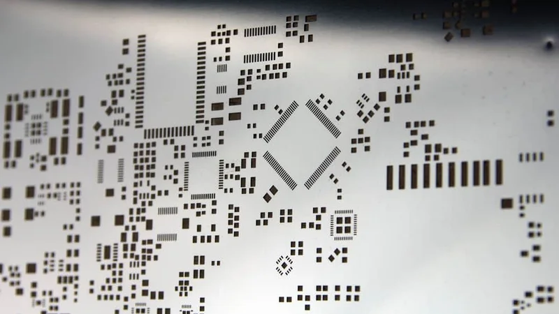
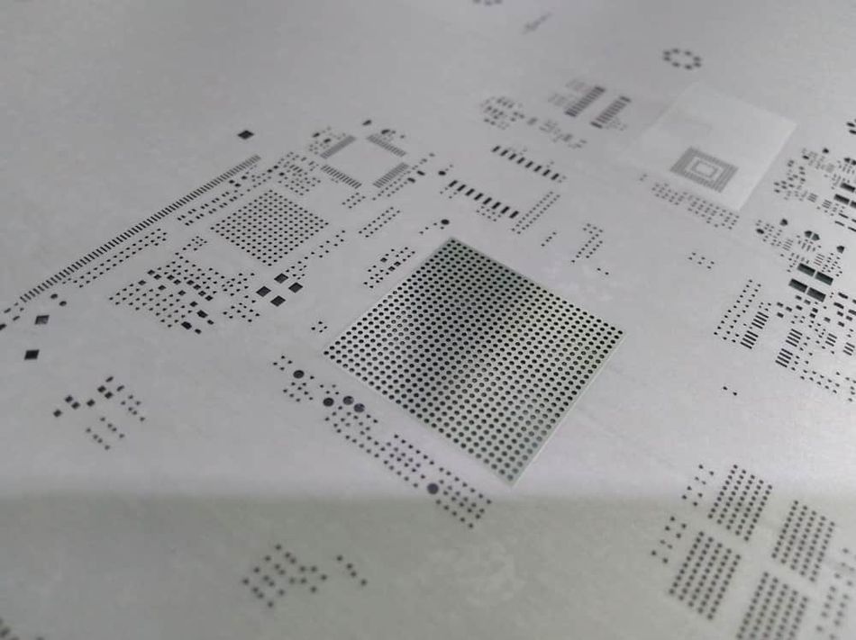
A typical PCB Stencil
What is a stencil in PCB?
A Printed Circuit Board (PCB) stencil is typically a thin sheet of stainless steel with openings that are generally laser-cut and is used for the application of solder paste to a circuit board to attach surface-mounted components. PCB stencils are utilised for solder paste coating over specific locations on the circuit board, which allows these components to be placed accurately in position and perfectly aligned. Its main purpose is to deliver the appropriate amount of solder paste to the surface-mount technology (SMT) pads to ensure that the joints are in perfect harmony with aspects of mechanical strength and electrical connectivity. They speed up the overall assembly process.
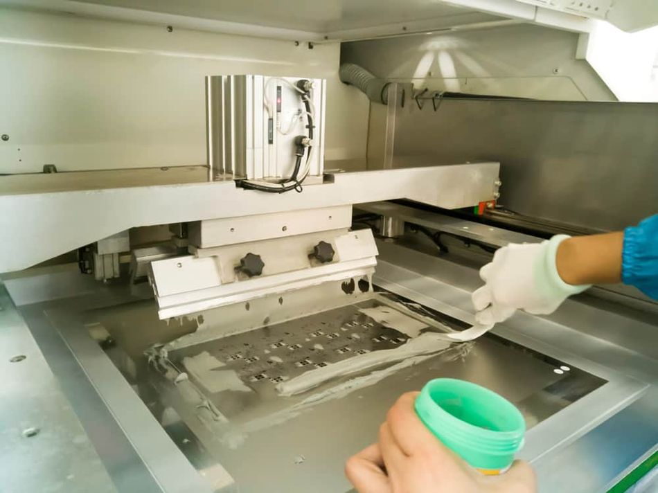
PCB stencils are broadly manufactured by incorporating stainless steel foil-based sheet metal plates with cutouts for surface mount components. The stencil is placed on the circuit board and perfectly aligned using registration points called fiducial marks. After alignment, the solder-paste is applied using a metal squeegee. Using the right PCB stencil when applying solder paste can speed up the PCB assembly process. It will also be easier and more accurate. The current and most widely used technology for soldering components onto a PCB is SMT.
What is a PCB Stencil made of?
Frame
Screen frames are majorly categorised into movable frames and fixed frames. The movable ones attach the steel plate directly to the frame, and the template frame can be used repeatedly. The fixed frame attaches the wire mesh to the formwork with an adhesive. A strong frame is easily achieved with a uniform steel tension, typically between 35 and 48 N/cm2. (Normal fixed frame allowable tension is 35N~42N).
Sheet
Copper plate, stainless steel plate, nickel alloy, polyester, etc. The stencil generally uses high-quality 301/304 stainless steel plates that have excellent mechanical properties, greatly increasing the service life of the stencil.
Mesh
The purpose of the mesh is to fix steel plates and formwork. There are two types of mesh; stainless steel and polymer polyester mesh. Stainless steel wire mesh is usually around 100 mesh to ensure a sufficient amount of stable tension. However, they tend to deform and lose tension when utilised for long periods. The organic fabric of polyester fabric, on the other hand, does not easily deform and has a long service life.
Glue
The glue is the binding material to attach the trellis frame and steel sheet. It plays a significant role in the template. The adhesive maintains strong adhesion and can withstand heavy cleaning with a variety of plate cleaners.
What are the different types of Stencils?
PCB stencils are classified by mounting type and opening type. Various PCB stencils, therefore, include Laser cut stencils, hybrid PCB stencils, chemically etched stencils, frameless PCB stencils, etc.
Framed SMT/PCB Stencil
It is supplied as a solder paste-stencil which has been laser-cut and then permanently attached to the frame. When attaching the stencil, use the edge of the net to taut the stencil foil within the frame. Framed stencils are designed for high-volume PCB screen printing. The template additionally processes a smooth opening that can be used with spacings of 16 mils or less. Ideal for stencil printing on high-volume printed circuit boards, using framed surface-mount technology, the stencil is double-bonded to oppose extreme wear and tear.
Frameless SMT Stencil
This type of stencil, also called the foil, is a laser-cut stencil designed to work with a reusable stencil frame known as the stencil clamp system. SMT stencil type that does not require permanent adhesion to the frame. Frameless SMT stencils are less expensive than framed stencils. And besides offering advanced quality and great performance, it also saves you money in terms of storage. It has a seamless open wall that can be used for 16mil pitch and below, especially micro BGA, and also has a 24-hour turnaround time standard.
Electroformed SMT Stencil
Electroformed SMT stencils or electroformed foils are nickel-based stencils permanently attached to a stencil frame by a mesh rim that stretches the foil within the frame. Electroformed stencils offer one of the best paste release attributes available. As a result, it is used in fine-pitch SMT applications (12 mils to 20 mil pitch) on printed circuit boards. It also applies to flip chips, wafer bumping, and µBGA (6 mils to 12 mil pitch). Additionally, the seamless trapezoidal sidewalls of the SMT stencil improve the solder paste application.
How are stencils manufactured?
All circuit-board stencils are made by forming openings or holes within a steel sheet or a foil. The process is assisted by lasers and the positioning indicates where the SMT components would be inserted. The stencil is placed on the surface of the PCB and perfectly aligned with the registration marks. The general process of stencil manufacturing consists of the following steps:
PCB Stencils process starts by cutting all the apertures in a stainless steel foil-base sheet using lasers precisely at the specified locations where Surface-Mount parts are required to be inserted.
After that, the stencil is positioned on top of the PCB and carefully positioned in perfect alignment using fiducial markings.
In the next step, a metal squeegee blade is used to apply the solder paste over the board after being aligned.
As a result, solder paste is applied to the PCB board where surface-mount components have to be installed.
Finally, components can be placed on the board once the stencil is removed.
There are three different methods utilised in manufacturing SMT stencils: chemical etching, laser cutting, and electroforming. Elecrow commonly utilises laser-cut templates. The data files needed to manufacture the laser-cut stencil should include the SMT paste layer, registration mark data, PCB outline layer, and drawing layer so that you can see both side data, component categories, etc.
Chemical Etching
This is a natural subtractive process that uses a chemical etching process to create openings. It can withstand all established standard cleaning procedures. Although relatively inexpensive as a process, it tends to produce poorer results (due to rougher orifice sidewalls).
Laser Cutting
Laser cutting is the most widely used method for stencil production. It also occurs as a subtractive process where the stencil sheet material is removed by laser cutting. Standard laser cutting often results in finer output, which helps achieve greater precision. It also provides a more consistent output or results compared to chemical etching processes. Note, however, that no moisture barrier is required as the process does not depend on the chemical environment.
Electroforming
This includes an additive process where stencil foils are developed by nickel electroforming. This process is also called his E-FAB. This process comes with a high cost of acquisition, but the price has been found to be independent of F-number in many cases. Additionally, any increase in processing time in this manufacturing or fabrication process is considered negative. It is available for all types of thickness and offers greater precision but incurs high initial costs and also requires greater processing time.
Do you need a PCB stencil?
Traditional PCB assembly processes require the manual placement of electronic components before soldering. However, the increasing complexity of electronic printed circuit boards, combined with the need for miniaturisation, necessitates mechanical assembly and solder paste application using SMT stencils. Placing and soldering many small components on a small circuit board is no longer practical.
Stencils replace the hand soldering of surface mount components and the inconsistencies caused by hand soldering. PCB Stencil creates repetitive solder marks and acts as a stencil to guide the application of solder paste to the PCB. Correctly placed and aligned on the circuit board. A runner then moves across the PCB stencil screen and pushes the correct proportions of solder paste into the holes in the PCB.
What is a stencil mask in PCB?
Paste mask layers are commonly referred to in the industry as stencils. SMD pads generally have the same or slightly smaller cavity size. This stencil is used in the SMD assembly soldering process to coat the SMD pads with tin paste. In the SMD (Surface Mount Device) welding process, the stencil is first covered on the circuit board (aligning the corresponding pads), then the paste is applied, the excess paste is removed with a blade, and then the stencil is removed. Make sure the solder pads are in place. Covered with paste. The parts are then attached with solder paste (either by hand or with a pick and place machine) and finally, his SMD assembly is completed with a reflow soldering machine. The stencil size is usually smaller than the actual weld pad on the PCB. A paste mask layer can also be split into a top paste and a bottom paste.
What is the difference between a solder mask and solder paste?
Solder Mask
A solder mask is a thin lacquer-like polymer layer that is usually applied to the copper traces of a circuit board to protect them from oxidation and prevent solder bridges from forming between the solder pads. Solder bridging is an unintentional electrical connection between two of her conductors by a small solder bump, and the board can prevent this with a solder mask. Solder masks are not always used for hand-soldered assemblies, but are important for mass-produced boards that are automatically soldered using reflow or solder bath techniques. An opening must be made in the solder mask wherever the component will be soldered after deposition. This is done using photolithography.
Solder Paste
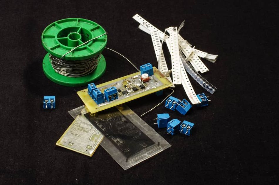
Solder paste, also called solder cream, is a mixture of small globules of solder contained in a special form of flux, the most important solder paste used to connect surface mount components in the manufacture of printed circuit boards. one of the ingredients. on the pads on the board. You can also solder through-hole pins to paste components by printing solder paste into the holes. Powdered metal solder suspended in a viscous medium called flux. Solder paste is a form of solder used in conjunction with infrared reflow machines during the PCB assembly process.
How to choose the correct stencil?
When choosing a stencil that would satisfy all your requirements, the following are some important points to keep in mind before ordering the desired PCB stencil:
Thickness of the stainless steel sheet
The precise thickness of the stencil sheet ensures that the required amount of solder paste is expelled from the opening. Board thickness and aperture size are important factors that affect the amount of solder paste applied to the board. This is because additional solder deposits can cause solder bridging. On the other hand, poor solder coverage can lead to weak solder joints and affect the functionality of the finished PCB.
Aperture size of the created opening created
The stencil opening is designed slightly smaller than the PCB pad size to avoid soldering defects such as bridges and solder balls. When the stencil is removed from the board after soldering, the solder paste can migrate to the board or stick to the walls of the stencil opening. To avoid this issue, the PCB pad area should always be greater than two-thirds of the area inside the stencil hole wall.
Stencil Material
The stencil material also affects the ability to transfer the solder paste from the opening/apertures to the PCB pads. Stainless steel is the material usually used for stencils. But other nickel-based materials can also be used for stencil production.
Stencil Alignment
Fiducial marks are added to both the PCB and the stencil to print perfect solder paste on the PCB pads. These registration marks ensure alignment between the circuit board and the stencil. If the surface-mounted parts are out of alignment, the functioning of the device can be impacted negatively. Therefore, the stencil alignment is important before proceeding to the paste application.
Key Takeaways
PCB stencils are essential tools for ensuring accuracy at every stage of PCB manufacturing. They are very helpful in keeping excess solder paste and other imperfections from building up that can prevent the circuit board from functioning properly. PCB designers and hobbyists need to understand the different types, what each means, and their application in the PCB development process. In addition, finding the right partner for your PCB assembly needs will help you get her PCB solder paste stencils suitable for your PCB assembly needs.
References
Admin. PCB Stencil: It’s Meaning and Importance in Circuit Board Production [Internet]. Hillman Curtis: China PCB Manufacturer and Assembly. 2021 [cited 2023 Jan 21]. Available from: https://hillmancurtis.com/pcb-stencil/
All about SMT stencil-Lioncircuits [Internet]. www.lioncircuits.com. [cited 2023 Jan 21]. Available from: https://www.lioncircuits.com/faq/pcb-assembly/what-is-a-smt-stencil-and-why-is-it-needed-for-assembly
Differences between Solder Mask & Paste Mask - ALLPCB.com [Internet]. www.allpcb.com. [cited 2023 Jan 21]. Available from: https://www.allpcb.com/soldermask/solder_mask_paste_mask.html#:~:text=Paste%20mask%20layer%20is%20generally
PCB Stencil FAQ | Using Circuit Board Solder Stencils - Sunstone Circuits [Internet]. www.sunstone.com. [cited 2023 Jan 21]. Available from: https://www.sunstone.com/pcb-products/pcb-solder-stencils/pcb-stencil-faq
What is a PCB Stencil and how to use it? [Internet]. www.elecrow.com. [cited 2023 Jan 21]. Available from: https://www.elecrow.com/blog/what-is-a-pcb-stencil-and-how-to-use-it.html
What is a PCB Stencil? - PCB Directory [Internet]. Pcbdirectory.com. 2021. Available from: https://www.pcbdirectory.com/community/what-is-a-pcb-stencil#:~:text=A%20PCB%20Stencil%20is%20a
What Is The Difference Between Solder Mask And Solder Paste? [Internet]. www.pcbgogo.com. [cited 2023 Jan 21]. Available from: https://www.pcbgogo.com/Blog/What_Is_The_Difference_Between_Solder_Mask_And_Solder_Paste_.html
in this article
1. Frame2. Sheet3. Mesh4. Glue5. Framed SMT/PCB Stencil6. Frameless SMT Stencil7. Electroformed SMT Stencil8. Chemical Etching9. Laser Cutting10. Electroforming11. Solder Mask12. Solder Paste13. Thickness of the stainless steel sheet14. Aperture size of the created opening created15. Stencil Material16. Stencil Alignment