What are Vias in Pad? Advantages, Limitations, Applications, and Comparison with Conventional Vias
Vias go through two or more layers of PCBs to form an electrical connection. Making them right under the component’s pad saves space, reduces track inductance and simplifies design.

11 Jan, 2023. 8 minutes read
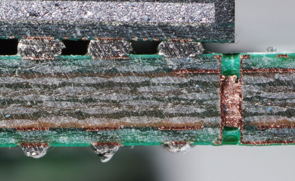
Vertical interconnect access (or via) are small electrical connections that enable the transfer of electrical signals between different layers of a Printed Circuit Board (PCB). If we consider the tracks to be present in the x and y axes of the board, vias exist in the z-axis. Structurally, they are just like tiny coated vertical pipes plated with a layer of conductive material (such as copper/gold) and placed in a drill hole. They are also filled with different substances to ensure good electrical conductivity and mechanical strength.
Traditionally, if a pin needs to be connected to a via, a track is made to route the signal away from its pad. However, the approach is inefficient for dense surface mount technology (SMT) PCBs and some Integrated Circuit (IC) packages like Quad-flat No Leads (QFN), and Ball Grid Arrays (BGAs).
In this article, we explain vias in pads. We introduce readers to the different types of commonly used vias and go on to discuss vias in pads in depth. We answer the most common questions around the topic and share a few key takeaways. After reading the article, you’ll be able to know:
- What is a via?
- What are the different types of vias?
- What are vias in pads?
- When to use vias in pads?
- What are the advantages and limitations of vias in pads?
- What are the differences between conventional PCB design and via in pad PCB design?
But before that, let’s quickly review the developments that led to the widespread usage of advanced electronic design techniques (such as vias).
Introduction
In the year 1965, Gordon Moore, the co-founder of Intel predicted that the number of transistors per silicon chip would double every two years or so. It was the beginning of a never-ending race that led to the consistent drop in the size of electronic components over the years to come.
The continued shrinking of electronic components and the invention of ICs in the 1980s rendered handmade circuit boards useless. This led to the development of PCBs which too had to evolve into multilayer, high-power, and flexible variants later to keep up with the pace.
PCBs provide mechanical support and a platform for circuit designers to place electronic components and connect them. While connecting components on a single-layer PCB can be done with the help of copper tracks, we need to use vias to transfer the signal from one layer to another.
What are the different types of vias?
Depending on the kind of connections made, vias can be classified into multiple different variants. Let’s take a look at some of the most commonly used ones.
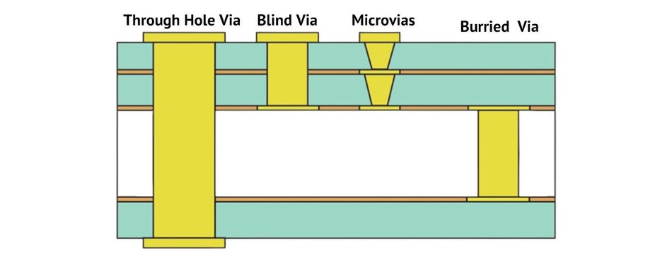
Through-hole via
Through-hole vias are used for shorting all the layers of the PCB at a given point. They are built by drilling a hole and coating it with a layer of copper (or conductive materials) to connect all layers starting from the top and going all the way to the bottom.
Through-hole vias are the most common type of vias in PCB manufacturing owing to their simple structure and construction. Among all vias, they are the cheapest and simplest ones to manufacture.
Advancements in precision machinery have led to the development of more sophisticated vias that let designers avoid certain layers of multilayer PCBs. Examples of specialized vias include blind via, buried via, microvia, and vias in pads.
Blind via
Blind vias are used for connecting the outer layers of a PCB to one or more of the inner layers. Since blind vias don’t go through the entire PCB, they can be seen from only one side of the PCB and are completely invisible from the other side. That’s how they get their name.
Compared to through-hold vias, blind vias are typically more complicated and expensive to build.
Buried via
Buried vias are used to connect two or more internal layers of the PCBs. Buried vias never touch the outer layers and hence are completely invisible from the outside. These vias can be made only on PCBs with four or more layers and are even more difficult to manufacture compared to blind vias.
Microvia
Microvias are miniature versions of traditional vias with some changes in their structure. Instead of being built in a cylindrical structure, microvias are built to resemble a frustum. As the via makes a transition from one layer to another, its radius keeps on decreasing.
For reliability issues, microvias are rarely made to connect more than two layers together. If a connection spanning multiple layers is required, microvias are stacked one on top of another. Buried microvias are generally filled with copper/conductive epoxy to improve their durability against mechanical stress and pressure.
Recommended reading: What is a via? A comprehensive guide
What is a via in pad?
Vias in pad are vias that are placed within an electronic component pad present on the surface of a PCB. They make a connection between the outer layer and the other layers of the PCB.

To understand the necessity of using vias in pad, let’s have a look at their application in High-Density Interconnect (HDI) and high-frequency PCBs having ICs with BGA packages.
Via in pad applications
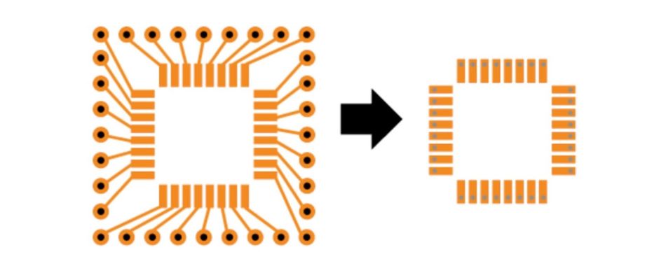
PCB designers use vias in pads when building PCBs where there isn’t enough space to accommodate traditional vias. They are often used with components in a BGA package as there isn’t much room for other vias in there.
BGA packages are used to permanently fix small-sized surface-mounted device (SMD) components having a large number of pins. Pins of components in BGA packaging are systematically arranged as a matrix with each pin having small solder balls. Compared to other commonly used packages such as dual-in-line (DIL) packages, BGAs offer higher packing efficiency and ruggedness.
The size of solder balls and the distance between nearby pins in BGAs can be as small as just a fraction of a millimeter which makes surface routing extremely complicated. Tracks with a very small trace width can be drawn out of each pin to a suitable place for making a via. But this isn’t the best approach.
In components where the distance between the pins is less than the safe track clearance will cause PCB design software to throw warnings.
As an alternative, instead of trying to route all pins away and making a via far from the component, vias can be made right below BGA pads to take the signal carried by the component’s pins to the required PCB layers.
What are the advantages of via in pad routing?
Here are some benefits of using vias in pad in-board design:
Space saving: As discussed in the previous section, one of the primary reasons for using vias in pads is to save space. Unlike traditionally built vias that require the signal to be routed away from the pad, vias-in-pads are directly made on the components’ pads leading to saving space. They eliminate the requirements of making dog-bone tracks which optimizes routing and drastically reduces the overall PCB footprint.
Easier routing: Letting designers place vias right under the pad not only frees up space but also makes routing simpler (especially for components having small footprints —such as the ones coming in the BGA package).
Improved heat dissipation: Vias in pads can significantly improve heat dissipation for the heat sources mounted on the PCB. Placing a via near a heat source improves the thermal conductivity between the components and the different layers of the PCB to allow heat dissipation at a faster rate.[1]
Reduced parasitic inductance: By eliminating the additional connection segment, vias in pads also reduce the parasitic inductance associated with them. Vias in pads also allow designers to place bypass capacitors close to their components which minimizes inductance. For high-speed designs and interfaces, this results in an improvement in signal integrity.
The Downsides of Via in Pad Technology
There are a few downsides of using vias in pads which need to be known beforehand to make an informed design choice. It’s always a good idea for PCB designers to review these points before opting for via in pad design.
Higher manufacturing cost: Creating vias in pads often requires more than just drilling a hole and coating with a conductive layer. Vias in pads have to be filled with either conductive epoxy or other conductive fillings to increase their mechanical strength. This increases the material costs and adds extra steps to the PCB assembly process. The fact that the costs of manufacturing vias in pads do not linearly scale down with an increase in the number of manufactured units further increases the associated costs.
Surface bumps: Surface bumps arise when the vias are not placed and filled precisely. These irregularities on the surfaces can complicate the process of soldering components (especially the smaller ones with a fine contact). Thus, when creating vias in pads, manufacturers must ensure all surface bumps are eliminated.
Increased design complexity: Vias in pad are difficult to design and implement.
Conventional Vias vs. Via in Pad PCB Design
Though implementing vias in the pad is very similar to implementing traditional vias from a functional perspective, there are a few key things that designers must keep in mind during the PCB design and manufacturing process. They are:
Verifying PCB manufacturer’s design capabilities: PCB manufacturers put up a description of the capabilities of their manufacturing process. Before going ahead and designing a PCB, designers must check the manufacturer’s website to understand different parameters like the minimal annular ring size to avoid design rule check (DRC) and design for manufacturability (DFM) problems at a later stage.
Extracting all the required files from the PCB design tool: Carefully reviewing the designs after exporting from the Electronic Design Automation (EDA) tools can solve many confusions and issues. In addition to the file containing a map of drills, supplying an additional file containing the map of just vias in pads ensures traditional vias don’t get capped or filled.
Via capping: Via tenting is a process of coating a via with solder mask to resist solder or solder paste. Since solder mask should not be applied to pads, via tenting is not an ideal solution for vias in pads. So, during the PCB fabrication process, manufacturers have to make a capped via under the pad to prevent solder from wicking into the via hole. There are some cases, for eg. when a via is placed below a thermal pad, it would dissipate heat much better if it is hollow and uncovered.
Recommended reading: Via tenting: Everything you need to know
Key Takeaways
Vias are used to transfer electrical signals between different layers of multi-layer PCBs. Instead of routing a signal away from a pin and placing a traditional via, vias can be made directly on pads. Making vias in pads saves space, simplifies routing, improves thermal management, and also reduces parasitic inductance. Vias in pads are typically more expensive than traditional vias. Designers must verify the design capabilities of their PCB manufacturer and ensure all required files are extracted from the PCB design tool to ensure their boards are manufactured without any hassle.
References
[1] Thermal Vias for Circuit Board Heat Management: Techniques and Tips, Cadence, [Online], Available from: https://resources.pcb.cadence.com/blog/2019-thermal-vias-for-circuit-board-heat-management-techniques-and-tips
[2]Via in Pad PCB Design, Macrofab, [Online], Available from: https://macrofab.com/blog/via-in-pad-pcb-design/