All you need to know about PCB Gold Fingers
Approximately 7% of the world's gold can be found inside discarded electronic devices, in form of PCB Gold Fingers. While a tonne of Gold Ore produces just 5 grams of pure gold on average, a tonne of electronic scrap can house 300 grams of gold inside it. Here we gloss over the significance of gold fingers in the present day electronics industry and all kinds of gold fingers specifications you need to know.

14 Jan, 2023. 9 minutes read
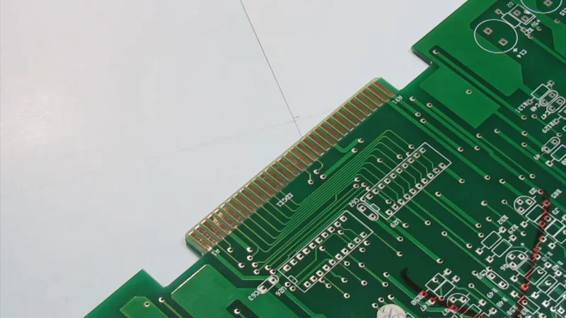
Gold Fingers are ubiquitous in all sorts of PCB boards.
Electronics prevail all around the globe today. Whether you visit a hospital, a government department, a school, a restaurant, or a supermarket, electronics are always running in the background. The backbone of this electronic connectivity is the PCB gold finger, a smart and witty invention responsible for today’s digitized landscape.
In general, electronic devices are not fully integrated into a single system. Rather, small electronic components are always linked together via contacts so that if a small component malfunctions, another one replaces it. And this is where PCB’s gold fingers come into the picture. For example, the central electronic in a computer (motherboard) may be connected to peripheral devices (speakers, microphones, monitors) with the help of the said gold fingers.
What are PCB Gold Fingers?
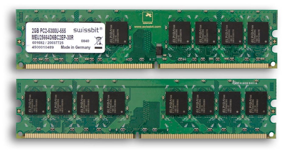
One might ponder over the nomenclature of these contacts. They are called “Gold Fingers” because they are long, thinly separated connectors that are made of gold. Gold is an unusually malleable metal with superior conductivity, and thus proves to be an ideal candidate for mass-scale production. The figure below shows a typical RAM memory used in computers, with gold fingers etched at its bottom.
We have two types of gold fingers available in the market, depending on the manufacturing process implemented while making them.
Electroless Nickel Immersion Gold (ENIG): The most commonly available gold fingers are created through this process as it is economical and relatively feasible to solder than electroplate gold. The drawback of this process is that it makes softer, thinner surfaces (2-5 Microns) which are prone to abrasion upon frequent mounting/dismounting.
Electroplated Hard gold: Considerably thicker films of Gold (generally 30 microns) can be achieved through this process but are reserved for specialized solutions considering higher manufacturing cost.
Gold fingers are the bridges of the computing industry, enabling all kinds of chips to communicate with each other via predetermined protocols. WiFi modules, RAMs, and processing units rely on undisturbed channels inside computer chips and then between different chips to execute commands.
For example, a button pressed on a TV device's remote control triggers a signal disseminated to one or more circuits. Then the PCB of the remote shoots signals through an LED blaster at the front of the remote, received by the IR receiver at the TV’s front. IR receiver sends the data to the main circuitry of the TV via gold fingers.
Gold Plating on a commercial scale requires several steps. To ensure reliability and performance, the gold plating conducted should be impeccable, and free of errors. Conforming to the standards also allows the contacts between the gold fingers of devices and the motherboard to be perfect fits.
It is essential to ensure that gold fingers always fit in the way they are intended to. For that, they usually undergo a few inspections. If the gold coated onto the material is worn away or the surface finish is not smooth, complications (or even safety hazards) can develop while using such a product.
During the manufacturing of a printed circuit board, all other processes are executed first, with the gold finger-plating process completed last.
How are PCB Gold Fingers used?
Gold fingers integrate two Printed Circuit Boards (PCBs) together. While electrical integration is the key objective here, the physical strength of the connection points is also important and that is where Gold comes into the picture. Hard Gold of specified thicknesses can be etched onto the PCBs in harsh industrial conditions. Hard Gold can retain its adhesiveness even after the PCB is mounted and dismounted 1000 times.
Gold Fingers are used today in three ways:
Interconnection points: PCI, ISA, or AGP slots connects the peripheral devices to the motherboard. Inside these slots lie gold fingers that connect the motherboard with memory cards etc.
Specialized adapters: Task-specific secondary PCBs are designed that are augmented into the main circuitry via gold fingers and aid the computer e.g. Graphics card. Being devices that stay assembled inside the CPU frame, the Gold Fingers of these devices are tremendously less prone to abrasion.
External connections: Gold fingers have allowed the connections to be established outside the CPU frame. A USB can be seamlessly connected/disconnected from a computer. Monitors, microphones, printers, and external Wi-Fi adaptors can be integrated at the front and back of the CPU tower, where secondary PCBs exchange data with external hardware before sending it back to the motherboard.
While the gold finger’s electrical conductivity is used for sending sensitive signals, it is also used to receive bulk electric power from the power supply and supply it to the circuits. Thus, different kinds of gold fingers are responsible for receiving electrical energy (in the power supply) and then utilizing the electrical energy (in the circuits).
The marvelous flexibility of PCB assemblies is also a factor why hardware is getting innovated with every new coming day. Hardware Industry is constantly coming up with new products because connecting newer components and discarding older components is really cheap and convenient. Obsolete graphics cards get removed and newer generations are attached to the same motherboards. Despite ever-increasing innovation in the hardware industry
Apart from the PC Industry, gold fingers are also used extensively in Computerized Industrial Machinery. Assembly plants, Mass manufacturing units as well as intelligent manufacturing machines all require extensive usage of PCBs.
In the health sector, many biomedical devices, are crucial for patients’ well-being. These devices constantly monitor patients’ vitals with other devices and alert the medical personnel in case of any anomaly. All of this is possible because of gold fingers that enable biomedical devices to monitor patients’ health, adjust the dosage, etc.
Automated manufacturing facilities cannot afford to be any lesser than perfect in terms of safety. In Assembling units where heavy presses and sharp drills operate tirelessly, safety concerns arise naturally. It is essential that sensors are reliable enough to detect safety threats in due time, communicating the safety threat to the main circuitry so that it can cease the operation of the tool that is likely to cause an accident. This is not possible until the communication between the sensors and PCBs is flawless. This is achieved by using the gold fingers of the appropriate grade.
Gold Finger Specifications
Gold fingers have a global demand in a versatile set of applications that necessitate different gold thicknesses, manufacturing specifications, and standards. From robotic arms to consumer electronics, gold finger technical specifications differ.
While designing gold fingers onto a specific PCB, certain specifications are kept in mind. These include the width of the finger, spacing between two gold fingers, alignment precision, finger length, and more. Even though the Gold fingers vary on a case-to-case basis, there are three golden rules that must always be obeyed:
Gold-plated connectors can not exist in the vicinity of a plated-through hole.
Solder Masks and screen printing should never be located close to the gold fingers.
In order to bevel the PCB edge, the gold fingers should never face in the direction of the middle of the PCBs.
Failure to comply with one or more of the above rules can cause defects in gold fingers leading to breakage of the connection of components with a circuit board or disfigured gold fingers that are unable to fit into the slots perfectly.
Gold is a very strong metal, which makes it a great candidate for an application that causes abrasion through continuous connecting/disconnecting. Not only that, it is a very malleable metal, complemented by phenomenal electrical conductivity. If some other metal may be used, the circuits may lose their contact with the friction. As if it was not already impressive, gold shows distinctive corrosion resistance as well as oxidation resistance, hailing as one of the least reactive metals in the reactivity series.
Is it possible to mass-manufacture PCBs without using the rarest element on earth? The simple answer is no, as the mechanical, electrical, and mechanical properties of rare earth metals are necessitated by modern-day architecture.
In order to further strengthen the gold, it is alloyed with nickel and cobalt before it is effectively electroplated. Nickel’s optimum thickness in the electroplating should lie between 150 microinches and 200 microinches.
In order to implement the standardization of Gold fingers all over the world, the Association Connecting Electronics Industries (IPC) was founded in 2002. Followed by the IPC-4556 (2012), the IPC A-600 and IPC-6010 were released in 2015 and now direct PCB manufacturing globally. Here is a brief outline of the IPC standards:
Chemical composition: Strength has to be ensured at the edge connectors of the PCB, and that is why cobalt should be added to the alloy mixture of Electroplating gold. The proportion of Cobalt should not be lower than 5 percent but must not exceed 10 percent.
Plating Thickness: Electroplating conducted for whatsoever application should not be thinner than 2 Microinches and should not exceed the thickness of 50 Microinches. Based on varying applications, Plating thicknesses are standardized as 0.031 inches, 0.062 inches, 0.093 inches, and 0.125 inches. Lower thicknesses are generally adopted in prototypes to conserve costs, while higher thicknesses belong to a class of PCBs where mounting/dismounting occurs on a routine basis.
Visual test: Visual test is a simple test that involves inspecting the Gold fingers for any potential defects with a magnifying lens. Edges should be given special attention during the inspection as they serve as the connection points between the devices. The surface finish of the edges should be smooth and should not have any excess plating deposited on them.
Tape test: Adhesiveness of the metal is as important as the surface finish of the electroplating, and that is why the tape test is conducted. A white strip of tape is placed along the edges and then pulled off. After the tape has been removed, it is observed for any signs of gold plating, the detection of which declares the product to be faulty.
PCB Gold plating can be broken down into three phases, which are executed after the solder masks and before the final surface finish. These three processes are:
Nickel Plating: The gold plating begins with a coat of nickel which is usually of a thickness of three to six microns of nickel.
Gold Plating: Hard Gold of two to three microns is deposited over the Nickel Plating. This Gold is alloyed with cobalt for boosted surface resistance and maximum rigidity.
Beveling: PCB gold finger beveling is a process of wedging the edges of the PCB for ease of insertion, aesthetics, and durability. Beveling is typically performed at 30 degrees but should not exceed more than 45 degrees.
Certain kinds of PCBs have gold fingers longer than others. This allows a PCB to insert into long slots. PCBs are pushed into the slot and snapped into place.
Plating of PCBs is a delicate procedure and requires some restrictions to be followed:
In order to avoid copper contact with air during the beveling process, inner layers have to be copper-free along the PCB edge.
Plated Holes and Plated pads have to be kept at a distance from the gold fingers, which is usually 1 mm.
Plated pads have to be kept under the maximum limit of 40 mm.
The edges and the gold fingers should be separated by 0.5 mm.
A PCB with gold fingers might become physically weak or stop working if the necessary gap around them is not spared.
Application of PCB Gold Fingers
PCB boards are the backbones of modern-day electronics and PCB boards drive energies into PCBs and enable them to communicate with each other. It is not possible to conceive today’s world without PCB Gold Fingers. While scanning a photo from a handheld device and sending it to a printer, many gold fingers have already been utilized for communicating between devices. They have not only made communication faster and cheaper but also reliable. Today, we see PCBs in all sectors of life including:
Medical Devices
LEDs
Consumer Electronics
Industrial Equipment
Automotive Components
Aerospace Components
Maritime Applications
Safety and Security Equipment
Telecommunications Equipment
Military and Defense Applications
Assembly houses
Personal Computers and more.
Key Takeaways
There was a time when computers were an organizational asset and not a device personal to every individual. With the advancement in hardware and software connectivity, older devices became obsolete only to be replaced by faster, more efficient devices. This was possible only because the process of integrating/disintegrating secondary PCBs was made much easier with the advent of Gold Fingers, and it is their feasibility to implement them that has made PCB Gold Fingers accepted as a global technology.
References
Gold Fingers [Internet]. Sierra Circuits. Sierra Circuits, Inc.; 2022 [cited 2023 Jan 12]. Available from: https://www.protoexpress.com/kb/gold-fingers/
MCL. PCB Gold Fingers – specifications & what you should know [Internet]. mcl. 2018 [cited 2023 Jan 12]. Available from: https://www.mclpcb.com/blog/guide-pcb-gold-fingers/
PCB Gold Finger Manufacturer [Internet]. PCBMay. 2021 [cited 2023 Jan 12]. Available from: https://www.pcbmay.com/pcb-gold-finger/
Wang J., Gold Finger PCB: A tough, durable contact edge for connecting PCBs [Internet]. PCB Assembly,PCB Manufacturing,PCB design - OURPCB. John Wang; 2022 [cited 2023 Jan 12]. Available from: https://www.ourpcb.com/gold-finger-pcb.html
Ultimate guide of PCB gold fingers and plating process updated in 2022 [Internet]. Pcbonline.com. [cited 2023 Jan 12]. Available from: https://www.pcbonline.com/blog/pcb-gold-fingers.html