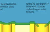
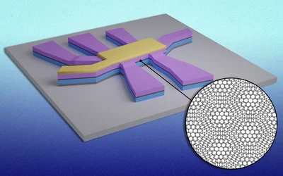
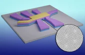
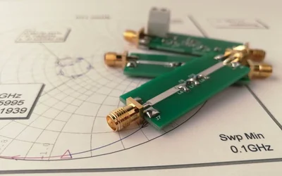
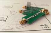
Be the first to know.
Get our Semiconductors  weekly email digest.

Semiconductors

featured

Printed Circuit Board Vertical Interconnect Access (PCB VIAs) are small plated holes that create electrical connections between different circuit board layers. This article delves into the various types, functions, and best practices of PCB VIAs to help you optimize your PCB design.

PCB Trace Width Calculator

Glossary of Semiconductors Terms

Featured

Wearable electronic textiles are a demanding environment for reliable interconnects – the ability to function with movement and survive multiple cleanings and reuse. Good adhesion is particularly challenging in these wearable and conformable electronics applications. While solders provide the most conductive electrical connection, they are rigid and require not only the addition of an underfill adhesive but usually a post bond encapsulation. This Anisotropic Conductive Epoxy, provides reliable interconnections between electronic components and circuitry on textiles with excellent structural bonding, without encapsulation, even under repeated stretching and washings. This technology has been shown as a scalable assembly process for e-Textile manufacturing in an SMT line.

Reliable, Scalable, Anisotropic Interconnect Solution for Wearable Electronics
Featured

Your new PCBA project design needs to pass production validation testing (PVT) to prove it's ready for production. The planning you did for cost, quality assurance, quality control, and scalability now positions your project for success.

Fab Insights: PVT in PCBA Product Development

Engineers Wiki.

Most Asked Questions.

Comprehensive Guide

View more

ORGANIZATIONS.

SHAPING THE INDUSTRY.

Nordic Semiconductor

Semiconductors

Nordic Semiconductor is a fabless semiconductor company specializing in wireless technology that powers the IoT.

181 Posts

MacroFab

EMS manufacturing

A better way to build electronics through a redefined experience, innovativ...

79 Posts

TechBlick

Electronics

TechBlick is a year round platform for onsite and online conferences, class...

65 Posts

OKdo

Appliances, Electrical, and Electronics Manufacturing

We’re OKdo, the global technology business from Electrocomponents Group. We...

37 Posts

Murata Electronics

Electrical and Electronics Manufacturing

Join the Innovators in Electronics.

37 Posts

View more

Miniature RFID tags by Murata enable seamless system integration with durable, reprogrammable identification — delivering reliable tracking, authentication & traceability beyond the limits of traditional barcodes.

How RFID Tags by Murata Boost System Integration

TAGGED WITH pcb

Latest Posts

Wearable electronic textiles are a demanding environment for reliable interconnects – the ability to function with movement and survive multiple cleanings and reuse. Good adhesion is particularly challenging in these wearable and conformable electronics applications. While solders provide the most conductive electrical connection, they are rigid and require not only the addition of an underfill adhesive but usually a post bond encapsulation. This Anisotropic Conductive Epoxy, provides reliable interconnections between electronic components and circuitry on textiles with excellent structural bonding, without encapsulation, even under repeated stretching and washings. This technology has been shown as a scalable assembly process for e-Textile manufacturing in an SMT line.

Reliable, Scalable, Anisotropic Interconnect Solution for Wearable Electronics

Your new PCBA project design needs to pass production validation testing (PVT) to prove it's ready for production. The planning you did for cost, quality assurance, quality control, and scalability now positions your project for success.

Fab Insights: PVT in PCBA Product Development

Wafer thinning is a part of the semiconductor manufacturing process. It is essentially grinding off the backside of the wafers to control their thickness and is useful for the production of ultra-thin wafers. These flattened wafers are used to effect stacked and high-density packaging in compact or microelectronic devices. This article discusses the meaning of wafer thinning, along with its various techniques and significance.

Wafer Thinning: Investigating an essential part of semiconductor fabrication

The progress of screen printing towards fine line printing has been incredible going from 100 µm features before 2010 to 70 µm to 2015 to 40 µm in 2018 and now pushing - in development- towards 20 µm and less. In parallel, the wet thickness of the printed line have gone down from 12um or so in 2018 to now just 4um.

The three themes are closely linked since QDs can be digitally printed as color conversation materials atop blue microLEDs to enable wide color gamut RGB uLED displays without requiring a separate transfer step for each color.. This is an important technology as it simplifies the manufacturing step for microLED and thus removing a major hinderence.

PCB layers are the copper layers within a printed circuit board, laminated between or onto layers of conductive material. These layers are stacked to enhance the functionality of electronic devices. This article explores the concept of PCB layering, the various types of layers, and their benefits.

PCB Layers: Everything You Need to Know