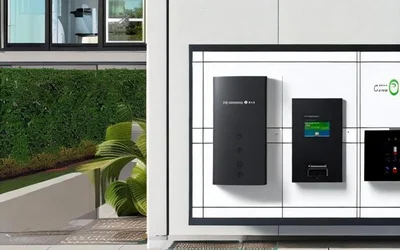
Category

Semiconductors

Latest Posts

The progress of screen printing towards fine line printing has been incredible going from 100 µm features before 2010 to 70 µm to 2015 to 40 µm in 2018 and now pushing - in development- towards 20 µm and less. In parallel, the wet thickness of the printed line have gone down from 12um or so in 2018 to now just 4um.

The three themes are closely linked since QDs can be digitally printed as color conversation materials atop blue microLEDs to enable wide color gamut RGB uLED displays without requiring a separate transfer step for each color.. This is an important technology as it simplifies the manufacturing step for microLED and thus removing a major hinderence.

PCB layers are the copper layers within a printed circuit board, laminated between or onto layers of conductive material. These layers are stacked to enhance the functionality of electronic devices. This article explores the concept of PCB layering, the various types of layers, and their benefits.

PCB Layers: Everything You Need to Know

Canadian researchers have discovered that they can stick hydrogel plasters to the skin very effectively using ultrasound. Outi Supponen has now explained the underlying mechanism: imploding bubbles that form within the adhesive located between the plaster and the skin anchor the one on the other.

Strong adhesion thanks to cavitation bubbles