Semiconductor Resilience with Innovations in Testing Techniques and Packaging
Advanced testing methodologies and innovation in semiconductor packaging ensure product reliability in dynamic and harsh operational environments. These strategies are particularly crucial in the rapidly evolving automotive industry.

21 Jun, 2023. 10 minutes read
Introduction
Semiconductors play a pivotal role in powering electronic devices, from smartphones and computers to automotive systems and industrial machinery. This article delves into the fascinating world of semiconductor testing, exploring its evolution, the changing operational environments, and the need for strict quality control measures. It seeks to provide an understanding of why comprehensive testing methodologies are crucial for maintaining a competitive edge in this rapidly progressing industry. Further, we look at the ways in which semiconductor company, Nexperia is setting industry standards for rugged manufacturing and testing processes, ,on the example of it`s clip-bonded FlatPower package CFP15B that passed the tough Board Level Reliability (BLR) specification at a leading Tier 1 supplier.
Understanding Semiconductor Testing
Semiconductor testing is a process designed to verify the electrical functionality of a chip or a device. It is a critical stage in semiconductor manufacturing, ensuring that the final product functions as per the specifications. From the earliest days of semiconductor technology, testing has played a vital role in maintaining quality and consistency.
Initially, semiconductor testing was relatively simple, often consisting of basic functionality and performance tests. However, as technology has advanced and semiconductors have become more complex, so too have the testing methodologies employed. Nowadays, tests are designed to evaluate numerous parameters, including performance under varying environmental conditions and lifetimes.
Current trends in semiconductor testing have been driven by demands for increased device performance, miniaturization, and energy efficiency, among others. Furthermore, the rise of new technologies, such as autonomous and electric vehicles, has created new challenges for testing, with requirements for high-speed, high-bandwidth, and low-power devices driving the development of novel testing techniques.
Types of Semiconductor Testing Techniques
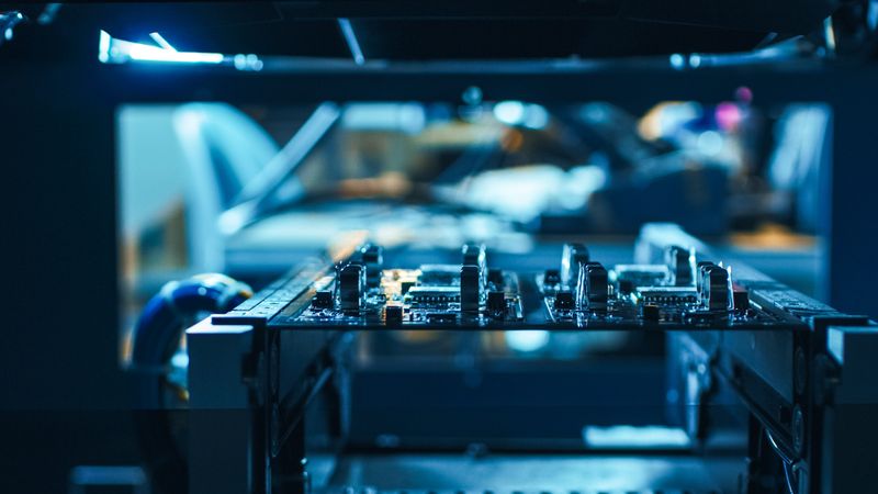
Robust testing methodologies are employed to ensure the ruggedness and reliability of semiconductors. Environmental testing is a fundamental part of these methodologies, where semiconductors are exposed to a range of extreme conditions to evaluate their performance and reliability under realistic environments. Examples of environmental tests include Temperature Cycling Test, High-Temperature Storage Life Test, Temperature Humidity Bias Test, Thermal Shock Test, and Burn-in Test.
Mechanical testing is essential to evaluate a semiconductor's ability to withstand physical stress. This includes testing for resistance to shock, vibration, and mechanical impact. Through mechanical testing, manufacturers can determine the robustness of their semiconductors and make design improvements as needed.
Various electrical tests, such as Current-Voltage (I-V) Characteristics Test, Gate Charge Test, Reverse Bias Test, Electrostatic Discharge (ESD) Test, and Lead Integrity Test, are also conducted to assess a semiconductor's ability to handle demanding operational conditions without compromising performance or reliability.
The AEC-Q101 Standard and Board-Level Reliability
The testing methodologies in semiconductor manufacturing have evolved to meet the increasing complexity of the products and the industry's stringent standards. AEC-Q101, for instance, has been seen as the gold standard for stress-test-driven requirements and conditions for discrete electronic components.
It ensures that electronic components used in automotive systems meet the rigorous demands of the automotive industry, including high temperature, humidity, mechanical stress, and electrical performance requirements. To comply with AEC-Q101, semiconductor manufacturers must subject their products to a series of tests and evaluations, including the initial product evaluation, reliability testing, and documentation of test results.
By adhering to these standards, manufacturers can ensure the reliability, durability, and safety of their components in the challenging automotive environment.
In recent times, newer testing methodologies, such as Board Level Reliability (BLR), have emerged. BLR testing assesses the robustness of semiconductor packages once they're soldered onto the printed circuit board. Boards are subjected to extreme bending, vibration, shock, and various other condition that may arise during operation. This is increasingly critical as electronics become more miniaturized, and the quality of the solder joints directly impacts the overall device performance and reliability.
Adapting to Changing Operational Environments in the Automotive Sector
As operational environments change, so too must semiconductor testing methodologies. For example, in the automotive sector, the emergence of e-vehicles and shared mobility is leading to increased drive cycles.
The average vehicle operates for 1.5 hours daily, or 8,000 hours over a 15-year lifetime. Under these conditions, 1,000 hours of reliability testing is typically sufficient. However, the operational profile changes dramatically for components like power semiconductors or Integrated Circuits (ICs) in electric vehicles, which interface with charging/battery circuits. These devices operate for around 8 hours daily (1-2 hours of driving and 6-7 hours of charging), resulting in 40,000 hours of operation over their lifetime. Consequently, they necessitate more than 4,000 hours of High-Temperature Storage Life (HTSL) reliability testing to ensure robust performance.[4]
Moreover, modern vehicles increasingly feature "always on" applications. They maintain a variety of functions even when turned off, such as radios, window, and door controls, and potentially cameras and fans for security and battery maintenance in electric vehicles. This constant activity significantly increases the operational hours for electronic components, intensifying the need for extended reliability tests.
Looking ahead, as autonomous vehicles become mainstream, the operational hours for numerous semiconductors could rise even further. This shift would further stretch reliability requirements, underscoring the necessity for advanced testing methodologies and more robust, high-performance packages.
In response to these changes, automotive Tier 1 suppliers are implementing more rigorous stress tests to evaluate semiconductor packages. The goal is to establish an industry standard that guarantees the robustness and reliability of semiconductors under these more demanding conditions. A significant development in this regard is the move beyond the AEC-Q101 testing standard.
Nexperia's Approach to Semiconductor Testing
Nexperia, a global player in the semiconductor industry, is responsible for shipping more than 100 billion parts each year. This translates to almost 300 million semiconductors every day. Despite their seemingly simple nature and modest cost, these components serve as the backbone of nearly every electronic design in the world. They are embedded in a vast range of applications, spanning automotive and industrial to mobile and consumer sectors.
Renowned for its unwavering commitment to premium product quality, Nexperia boasts an impressively low product failure rate, measured in single-digit parts per billion—a testament to their successful quality control measures. This achievement reflects their rigorous quality policies and the ambitious goal of attaining zero customer incidents. As an industry leader, Nexperia recognizes the essential role of quality control and constantly refines its testing methodologies to confront the evolving operational environments with confidence.
In direct response to the dynamic requirements of the automotive industry, Nexperia has boldly transcended the confines of the traditional AEC-Q101 stress test standard. The company has integrated exceptionally rigorous testing procedures for numerous products, such as BLR, into its comprehensive quality assurance process.
By continually raising the bar for semiconductor testing, Nexperia ensures the performance of its own parts but also helps set a higher standard across the industry. This commitment to exceeding rather than merely meeting industry standards serves as an example of how companies can contribute to advancing the field and bolstering the reliability of electronic systems worldwide.
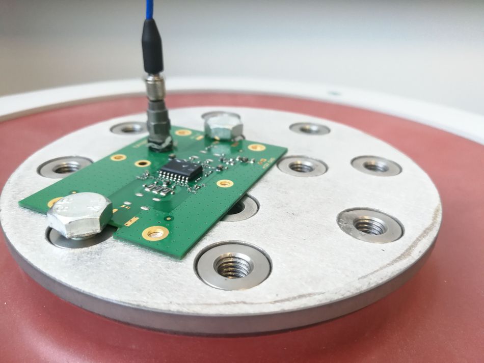
Advancements in Packaging: CFP15B/SOT1289B
Nexperia's CFP15B (CFP: Clip-bond Flat Power) package, also referred to as SOT1289B, is a part of their range of four CFP packages. These packages are designed to meet the challenging demands of efficient and space-saving designs, making them a high-performance alternative to previous-generation Surface Mount Technology packages such as SMA, SMB, and SMC (SubMiniature versions).
CFP packages are used by various power diode technologies, such as Nexperia’s Schottky, Silicon Germanium, and recovery rectifiers, and the CFP15B package can also be extended to bipolar transistors. They provide significant product diversity, covering single/dual configurations, thereby simplifying board design. These packages are suitable for a wide range of applications, including automotive, industrial, consumer, and computing applications.
Addressing these evolving requirements for increased robustness, Nexperia's CFP15B clip-bond FlatPower package has emerged as a front-runner. The CFP15B package has demonstrated exceptional ruggedness, passing BLR testing at a leading Tier 1 supplier for the first time. This is particularly significant as it assures automotive engineers of the package's capability to withstand the harsh conditions typical of new operational environments, such as those found in an engine control unit.
Extended reliability test based on AEC-Q101 | Standard | Test condition | Standard AEC-Q101 | Beyond AEC-Q101 qualification |
HTRB High-temperature reverse bias | JESD22-A108 | T=T jmax VR > 80% of max. breakdown voltage | 1000 h | Up to 4000 h |
TCT Temperature cycling | JESD22-A104 | -55°C to Tjmax | 1000 cycles | Up to 4000 cycles |
IOL Intermittent operating life | MIL-STD-750 method 1037 | ton = toff, device powered to ensure ΔTj 100°C | 1000 h | Up to 4000 h |
HTS High temperature storge |
| Tamb=150°C | 1000 h | Up to 4000 h |
Table 1: Testing standards adopted by semiconductor companies go beyond AEC-Q101[2]
CFP15B, with its high-quality construction and design innovation, can operate optimally under strenuous conditions. In a specific instance, the package demonstrated twice the level of reliability performance expected per the AEC-Q101 standard. The CFP15B package achieved a qualification of 2,600 cycles during power temperature cycles, which combined temperature cycling and intermittent operating life tests.
The Pillars of CFP15B’s Performance: Design Innovation and Material Quality
The performance of the CFP15B package is underpinned by design innovation and the use of high-quality materials. The package features a solid copper clip which significantly reduces thermal resistance compared to wire-bonded packages such as Discrete or Decawatt Package (DPAK). This ingenious feature enhances the transfer of heat into the PCB, accommodating smaller PCB designs without compromising thermal behavior.
Moreover, the CFP15B package is compact and ultra-thin. In fact, it is up to 60% smaller than DPAK and SMx packages. This smaller size offers automotive design engineers space-saving options and consequently greater design flexibility. The package also eliminates moisture ingress by providing zero delamination in areas such as around the leads, die, and clip. This enhances performance reliability, a critical feature for components operating in stringent environments.
Key features and benefits of the CFP15B clip-bond FlatPower package include:
- A solid copper clip for high thermal performance and power dissipation.
- Reduced package inductance for improved switching behavior.
- High reliability, being compliant with twice the AEC-Q101 standard and Board Level Reliability.
- Freedom from delamination.
- Junction temperature support up to 175 °C.
- A small, thin, and light design.
- Optimized lead form, ensuring uniform solder joints for maximum flexibility in AOI (Automated Optical Inspection).
- Secure supply in high volumes.
Envisioning the Future of Semiconductor Component Reliability
The automotive sector's metamorphosis is propelling a sea of change in the supply chain. With vehicles progressively adopting electric and connected functionalities, there is an escalating demand for enhanced power electronics. These are not limited to the primary propulsion motor control and battery management systems but extend to sensors, networking, communications, and satellite navigation. With this growing demand, the necessity for robust, high-power packages is rising, prompting the quality thresholds to advance beyond existing standards such as AEC-Q101.
Nexperia stands at the forefront of this exhilarating digital revolution in the automotive industry. The company demonstrates an unwavering commitment to delivering tried-and-tested, future-proofed packages that are not only rugged but also space-efficient and versatile, thus making them ideal for high-reliability applications.
Conclusion
The relentless expansion of electronic products, propelled significantly by the automotive industry's evolution, necessitates increasingly reliable and efficient semiconductors. Companies leading the industry are meeting this call to action with versatile, high-performance package technologies that not only meet but often surpass rigorous reliability tests, setting new standards for the semiconductor field.
Nexperia is working to advance semiconductor testing to achieve superior performance and reliability while simultaneously challenging industry norms with its innovative packages, such as the CFP15B clip-bond FlatPower package. These developments underline the significance of quality and reliability in a world where technology is rapidly relied upon for mission-critical applications.
About the sponsor: Nexperia
Headquartered in the Netherlands, Nexperia is a global semiconductor company with a rich European history and over 15,000 employees across Europe, Asia, and the United States. As a leading expert in the development and production of essential semiconductors, Nexperia’s components enable the basic functionality of virtually every electronic design in the world – from automotive and industrial to mobile and consumer applications.
The company serves a global customer base, shipping more than 100 billion products annually. These products are recognized as benchmarks in efficiency – in process, size, power, and performance. Nexperia's commitment to innovation, efficiency, sustainability, and stringent industry requirements are evident in its extensive IP portfolio, its expanding product range, and its certification to IATF 16949, ISO 9001, ISO 14001, and ISO 45001 standards.

References
[1] "Nexperia. Clip-bond FlatPower package - CFP15B/SOT1289B [Internet]. Nexperia; [cited 2023 May 23]. Available from: https://www.nexperia.com/packages/SOT1289B.html"
[2] ‘Nexperia's Webinar Package Technology for Electronic Design Engineers’ [Internet]. YouTube; 2023. Available from: https://www.youtube.com/watch?v=zFY_EWuSg5M
[3] Meet automotive Board Level Reliability (BLR) requirements with Nexperia’s CFP15B Package [Internet]. YouTube; 2022. Available from: https://www.youtube.com/watch?v=7bLJ4VT4YgQ
[4] Prasad Dhond’s Linkedin Post, LinkedIn; 2023, Available from: https://www.linkedin.com/posts/prasaddhond_why-do-automotive-customers-demand-2x-or-activity-7061671158659600384-epz8