Featured
Exploring Silicon Photonics: Shaping the Future of Optical Communication
Exploring Silicon Photonics: Shaping the Future of Optical Communication
PCB Trace Width Calculator
Glossary of Semiconductors Terms
Exploring Silicon Photonics: Shaping the Future of Optical Communication
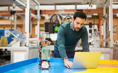
In response to the OKDo Engineering Challenge provocation, a team from the University of Maribor submitted a proposal to use the ROCK 5B in their raspberry detection and localization robot.
There are times when scientific progress comes in the form of discovering something completely new. Other times, progress boils down to doing something better, faster, or more easily.
Semiconductors are the building blocks of modern electronics, powering everything from smartphones to satellites. This in-depth guide provides a comprehensive understanding of semiconductors' engineering principles and applications, delving into their fundamental concepts, materials, devices, manufacturing processes, and their impact on today's technology landscape.
13 minutes read.
20 minutes read.
16 minutes read.
20 minutes read.
20 minutes read.
13 minutes read.


Semiconductors
Nordic Semiconductor is a fabless semiconductor company specializing in wireless technology that powers the IoT.
181 Posts
A guide covering the full radio-frequency design workflow, starting from setting specifications and choosing topologies to matching, simulation, layout, and verification, to help antenna engineers.
This article presents a detailed technical exploration of SiC MOSFET devices, covering material physics, device structure, switching behavior, and practical design considerations for high-efficiency power electronics systems.
This article is a comprehensive technical guide to relay wiring diagrams, covering 4-pin and 5-pin configurations, working principles, safety practices, standards, and advanced relay applications in modern systems.
Explore how frequency shapes EMC behavior from RF emissions to ultra-low-frequency drift, with mitigation strategies for robust, compliant electronic system design.
How Essentra Components Supports Engineering from Concept to Production
Makera gives live demonstrations of the Z1 during the 2026 Hackaday Europe event. The Z1 is a compact CNC manufacturing platform.
A crystal oscillator is an electronic circuit that uses a quartz crystal to produce a precise and stable frequency reference. This article covers crystal operation, equivalent circuit models, resonance, load capacitance, oscillator topologies, stability, aging, and design practices.
June 25, 2026 at 08:00 PM Central European Summer Time
Exploring Silicon Photonics: Shaping the Future of Optical Communication
In response to the OKDo Engineering Challenge provocation, a team from the University of Maribor submitted a proposal to use the ROCK 5B in their raspberry detection and localization robot.
There are times when scientific progress comes in the form of discovering something completely new. Other times, progress boils down to doing something better, faster, or more easily.

4 minutes read
Radio Frequency Identification (commonly known as RFID) is a technology that leverages wireless communication over radio waves to both transfer data and locate objects.

4 minutes read
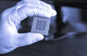
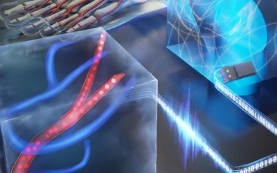
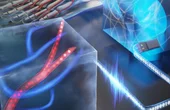
Transistors — the tiny on-off switches inside microchips — have gotten smaller and smaller over the years, increasing computing power and enabling smaller devices. During that time, the copper wires that connect these switches have likewise shrunk.

2 minutes read
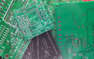
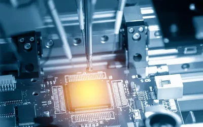
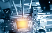
Two primary PCB assembly techniques have emerged as the electronics industry standards: Through-Hole Technology (THT) and Surface Mount Technology (SMT). This article delves into the intricacies of THT and SMT, providing a thorough comparison of their advantages, disadvantages, and applications.
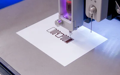
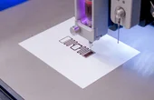
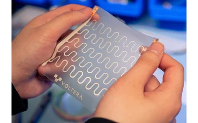
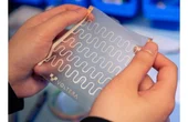
Exploring the transformative journey of flexible electronics and how additive manufacturing is the future.
Learn how SBCs take advantage of the different operating systems and ensure stability and robustness in different applications
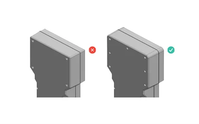
Designing waterproof enclosures for electronics is a blend of choosing the right materials, like ABS, and paying attention to details.
Interview with Misha Govshteyn, the CEO of MacroFab and Brenden Duncombe, the Director of Customer Engineering.
Sponsor interview with Theresa Hackl, Application Marketing Engineer, Komei Takura, Senior Business Development Manager for Mobility and Yoichi Murakami, Senior Product Manager for Function Devices at Murata.
Sponsor interview with Mark Patrick, the Director of Technical Content, EMEA at Mouser Electronics.
How Single Board Computers (SBCs) have automated and reduced costs in modern agriculture
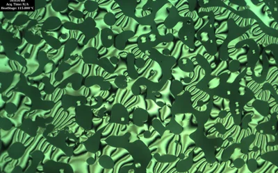
A new study led by chemists at the University of Illinois Urbana-Champaign brings fresh insight into the development of semiconductor materials that can do things their traditional silicon counterparts cannot – harness the power of chirality, a non-superimposable mirror image.

2 minutes read
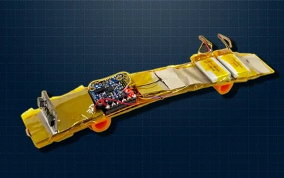
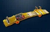
Princeton researchers have developed a flexible, lightweight and energy efficient soft robot that moves without the use of any legs or rotary parts. Instead, the device uses actuators that convert electrical energy into vibrations that allow it to wiggle from point to point using only a single watt.