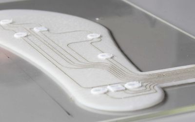
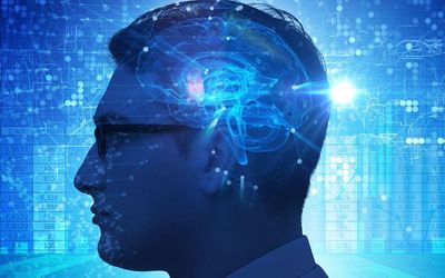
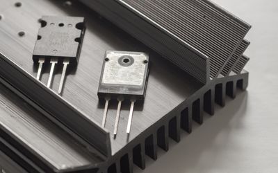
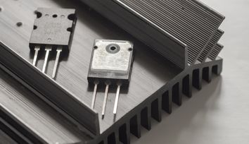
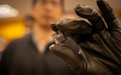
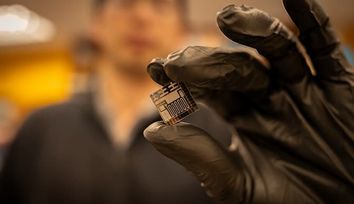
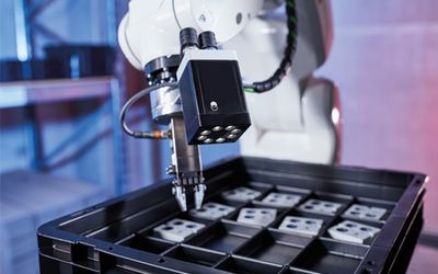
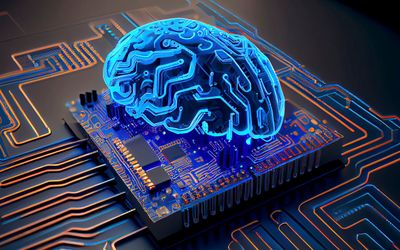
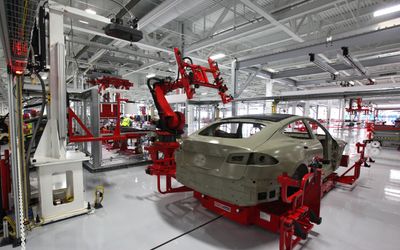
Be the first to know.
Get our Electronics  weekly email digest.

Electronics

ORGANIZATIONS.

SHAPING THE INDUSTRY.

Mouser Electronics

Electronics

Mouser Electronics is a worldwide leading authorized distributor of semiconductors and electronic components.

219 Posts

MacroFab

EMS manufacturing

A better way to build electronics through a redefined experience, innovativ...

79 Posts

TechBlick

Electronics

TechBlick is a year round platform for onsite and online conferences, class...

65 Posts

Xsens

Appliances, Electrical, and Electronics Manufacturing

Xsens digitizes movement.

47 Posts

Murata Electronics

Electrical and Electronics Manufacturing

Join the Innovators in Electronics.

37 Posts

TAGGED WITH microchips

Latest Posts

A new method for the miniaturisation of biosensors will enable new possibilities for minimally invasive implants. The miniaturised transistors are fabricated on thin, flexible substrates, and amplify biosignals, producing currents more than 200 times larger than analogous alternatives.

Miniaturised biosensors for minimally invasive implants

PCBs are extensively used across industries, powering devices from simple gadgets to complex systems. In this article, we’ll understand the importance of PCB thickness, the various factors affecting it, and its impact on design and other factors.

Understanding PCB Thickness: A Comprehensive Guide

Human activity, from climate change, pollution, and habitat destruction, to poaching, territorial conflict, and trophy hunting, has seen the IUCN’s list of endangered species balloon to more than 147,000 in recent years, with 41,000 species threatened with extinction.

Endangered wildlife has wireless lifeline

A unique new approach of printing functional materials with unparallel precision and repeatability. Technology called Ultra-Precise Deposition (UPD) is a nanodispensing method capable to print high density and high viscous materials with the resolution down to 1 µm in feature size and with high ratio of width to height after single pass. For this method material extrusion is controlled by a pressure, which means it is not supported with high electric field. Thanks to this there are no limitation if the substrate is conductive or dielectric.

Ultra-Precise Deposition for the Fabrication of Next-Generation MicroLED and QD-LED Displays

PCB traces are fundamental components in circuit design, serving as the pathways for electrical signals. This article examines the advancements, applications, and challenges of PCB trace technology. Discover insights into optimizing designs and overcoming common obstacles in PCB trace implementation.

PCB Trace: The Backbone of Modern Circuit Design